Symmetrical ULF made from available parts based on V. Korol
Analysis of letters from radio amateurs allowed us to come to the following conclusions. Firstly (and this is natural), everyone is in favor of creating simple circuitry AF power amplifiers (UMZCH); secondly, the simpler the amplifier circuit, the less trained radio amateurs undertake its assembly; thirdly, even experienced designers often ignore known installation rules, which leads to failures when repeating UMZCH on a modern element base.
Based on the above, the UMZCH was developed (see Fig. 1). Its main features are the use of op-amps in small-signal mode, which expands the frequency band of signals reproduced without exceeding the slew rate of the op-amp's output voltage; transistors of the output stage - in the OE circuit, and the pre-terminal stage - with a divided load in the emitter and collector circuits. The latter, in addition to the obvious design advantage - the possibility of placing all four transistors on a common heat sink, provides certain advantages compared to the output stage in which the transistors are connected according to the OK circuit.
Main technical characteristics of UMZCH:
Nominal frequency range with frequency response unevenness 2 dB: 20 – 20000 Hz
Rated output power into 4 ohm load: 30 W
Maximum output power into a 4 ohm load: 42 W
Rated output power into 8 ohm load: 15 W
Maximum output power into 8 ohm load: 21 W
Harmonic coefficient at rated power in the rated frequency range: no more than 0.01%
Nominal (maximum) input voltage: 0.8 (1) V
Input impedance: 47 kOhm
Output impedance: no more than 0.03 Ohm
Relative noise and background level: -86 dB
Amplitude of output voltage surges when turning the UMZCH on and off: no more than 0.1 V
Op-amp DA1 is powered through transistors VT1 and VT2, which reduce the supply voltage to the required values. The quiescent currents of the transistors create voltage drops across resistors R8 and R9, sufficient to provide the required bias voltage at the bases of transistors VT3, VT4 and VT5, VT6. In this case, the bias voltages for the transistors of the final stage are chosen such (0.35...0.4 V) that they remain reliably closed when the supply voltage increases by 10...15% and overheating by 60...80 °C. They are removed from resistors R12, R13, which simultaneously stabilize the operating mode of the transistors of the pre-final stage and create local negative feedback on current.
The relationship between the resistances of resistors R11 and R4 of the OOS circuit is selected from the condition of obtaining a nominal input voltage of 0.8 V. The inclusion of external correction and op-amp balancing circuits is not shown in the diagram for simplicity (this will be discussed in the section devoted to setting up the amplifier).
Low-pass filter R3C2 and high-pass filter C3R10 with cutoff frequencies in the region of 60 kHz prevent the operation of relatively low-frequency transistors VT3-VT6 at higher frequencies in order to avoid their breakdown. Capacitors C4, C5 correct the phase response characteristics of the pre-terminal and final cascades, preventing their self-excitation if installation is unsuccessful.
Coil L1 increases the stability of the UMZCH with a significant capacitive load.
The UMZCH is powered by an unstabilized rectifier. It can be common to both channels of the stereo amplifier, but in this case the capacitance of filter capacitors C8 and C9 must be doubled, and the diameter of the wire of the secondary winding of transformer T1 must be increased by 1.5 times. Fuses are included in the power supply circuit of each amplifier.
The design of the UMZCH can be different, but some design features on which the success of its repetition depends must be taken into account.
Printed circuit board drawing and placement of parts for one UMZCH channel
are shown in the figures:
The length of the leads of the parts should be no more than 7...10 mm (for ease of installation, the leads of the op-amp DA1 are shortened to approximately 15 mm). In UMZCH it is necessary to use ceramic capacitors with a rated voltage of at least 50 V. The board can be mounted on the heat sink of the transistors of the final stage using racks 15...20 mm high or in close proximity to it, using any detachable connector to connect the final stage to the pre-terminal one, for example MRN-22 (sockets and connector pins are connected at points 1-5). In the latter case, the resistance of resistors R12 and R13 should be selected equal to 43...47 Ohms, and on the connector socket with transistors VT5, VT6 connected to it, resistors of the same resistance R12′ and R13′ should be installed (this will prevent failure of the transistors if contact is lost in the connector ). The length of the conductors between the board and the transistors of the final stage should be no more than 100 mm.
In addition to what is indicated in the diagram, the UMZCH can use op amps K140UD6B, K140UD7A, K544UD1A, however, the harmonic coefficient at frequencies above 5 kHz will increase in this case to approximately 0.3%.
The transistors of the pre-terminal stage are placed on a heat sink, bent from a plate with dimensions of 70X35X3 mm (excluding a tab with a hole with a diameter of 2.2 mm) made of aluminum alloy, which is attached to the board with one M2X8 screw and nut to prevent breakage of the transistor leads during accidental mechanical impacts.
The transistors of the final stage can be placed either on a heat sink common to each channel of the UMZCH, or on a heat sink common to both channels. In the first case, they are fixed to the heat sink and the latter is isolated from the UMZCH case; in the second case, the transistors are isolated, and the heat sink can be a structural element of the amplifier case. To reduce the thermal resistance of the transistor body - heat sink, it is necessary to use thermal conductive paste. When using separate (for each channel) heat sinks, you can use transistors in a plastic case, which, due to the small area of the metal bases, can overheat if the gaskets are poorly made or the thermal contact with the heat sink is loose and there is an excessive amount of paste in the gap. It is advisable to install transistors in a metal case on a heat sink common to both channels. The heat sink area per transistor must be at least 500 cm2.
The installation of the UMZCH and the connection of its channels to the power source are of great importance. The power wires (+22 V, -22 V and common) should be as short as possible (they should be laid separately for each channel) and of a sufficiently large cross-section (with a maximum power of 42 W - at least 1.5 mm2). Wires of the same cross-section must be used to connect the speaker systems, as well as the emitter and collector circuits of the final stage transistors to the UMZCH board.
They set up the UMZCH with the final stage turned off. If a detachable connector is used to connect parts of the UMZCH, it is convenient to use a technological socket to which only the power wires and the output of the AF signal generator are connected. When directly connecting the terminal transistors to the UMZCH board, it is enough to remove the solder jumpers from the printed conductors of their base circuits and temporarily solder the latter to the emitter terminals.
To balance op-amp DA1 (if the need arises), the board has holes for trimmer and fixed resistors or wire jumpers to connect the pins of the microcircuit in accordance with the balancing circuit for a specific type. For example, to balance the K544UD2 op-amp, its terminals 1 and 8 are connected through a resistor with a resistance of 62 kOhm to the output of the engine and one of the terminals of the resistive element of a trimmer resistor with a resistance of 22 kOhm. The free terminal of this resistor is connected by a wire jumper to pin 7 of the op-amp, and through a resistor with a resistance of 75 kOhm to pin 5 (in Fig. 2 these elements are shown with dashed lines). When using the K544UD1 op-amp, its pin 1 is connected through a resistor with a resistance of 4.3 kOhm to the terminals of a trimming resistor with a resistance of 1.5 kOhm. Its free pin is connected to pin 8 of the op-amp through a resistor with a resistance of 5.1 kOhm, and to pin 7 with a jumper wire. To balance the op-amps K140UD6 and K140UD7, resistors of the same values are used, but the free output of the adjusted resistor is connected through a constant resistor to pin 5, and by a jumper to pin 4 of the op-amp. However, balancing may not be necessary, so these parts are installed only if necessary.
The setup begins with the input of the amplifier being short-circuited, an oscilloscope turned on in maximum sensitivity mode is connected to the output, and power is applied briefly. If there is no alternating voltage at the output, i.e. there is no self-excitation, measure the operating mode of transistors VT3, VT4 and op-amp DA1 using direct current. The op-amp supply voltages should be within the range of +13.5...14 and -13.5...14 V and be approximately the same (deviation is acceptable within 0.2...0.3 V). The voltage drop across resistors R12 and R13 should be equal to 0.35...0.4 V. If they differ significantly (by more than 10%) from the specified value, it is necessary to select resistors R8, R9, making sure that their new resistance remained the same. Replace resistors when the UMZCH power is turned off. The approximate resistance of resistors for the K544UD2A op-amp is indicated in the diagram. When using op-amps K544UD1A and K140UD6, their initial resistance should be 680 Ohms, and when using K140UD7 - 560 Ohms.
Having selected resistors R8, R9, measure the DC voltage at the output of the UMZCH and, if it exceeds 20...30 mV, balance the op-amp DA1. Then connect the bases of transistors VT5, VT6 to the emitters VT3, VT4 and, briefly turning on the power, make sure that even in this form the UMZCH does not self-excite. The AC noise and background voltage when the input is short-circuited should not exceed 1 mV.
Next, a resistor with a resistance of 16 Ohms with a dissipation power of 10...15 W is connected to the output of the UMZCH, the input of the UMZCH is opened, a generator tuned to a frequency of 1 kHz is connected to it and, gradually increasing its signal until a voltage of 13.5...14 V is obtained at the load, the symmetry is checked limitations of positive and negative half-waves of a sine wave.
The minimum (within the specified limits) constant voltage at the output of the amplifier is achieved, if necessary, by final balancing of op-amp DA1. After this, you can begin to measure the main characteristics of the UMZCH by loading it with a nominal load - a resistor with a resistance of 4 or 8 Ohms.
It should, however, be taken into account that an attempt to adjust, and even more accurately evaluate the parameters of a UMZCH assembled without observing the above installation rules, without installing it in the place intended for it and without powering it from its own power supply, will not only not give the desired result, but it can also lead to failure of the output stage transistors. Setting up the UMZCH and measuring its characteristics should be started only after its design has been completely completed. The simplicity of the amplifier is only apparent. We should not forget that both the DA1 op-amp and the UMZCH as a whole use transistors with maximum generation frequencies of 100...300 MHz, and in the output stages - with significant transition capacitances, which can lead to self-excitation even in the apparent absence of feedback circuits and loads of sufficient magnitude. The insignificant inductance of the emitter circuit wire, the parallel arrangement of the base and collector circuit wires over a significant length can cause self-excitation at high frequencies, which is extremely dangerous for transistors of the final and pre-terminal stages. (However, this is true not only for the device described, but also for UMZCH assembled according to any other scheme.)
When measuring the harmonic coefficient and the relative level of noise and interference, you should remember about possible interference from the power supply network, television and radio transmitters, televisions and other radio devices due to poor shielding of connecting wires, the UMZCH input and sensitive measuring instruments, as well as in the absence of their connection ungrounded enclosures to each other. Sometimes it is enough to rearrange the power plug of one of the devices or UMZCH in the socket to get the wrong result. By the way, you should not use the method of checking the UMZCH, known from old amateur radio practice, by touching its input circuit with your finger. This can lead to such a level of high-frequency interference that the output transistors fail.
The considered circuit can be taken as a basis when creating UMZCH with different output powers. To do this, you just need to change a number of elements of the UMZCH and the power supply. Some recommendations on this matter can be gleaned from the table. When constructing a UMZCH with an output power of approximately 25 W, some elements can be eliminated (see Fig. 3). As you can see, instead of a resistor in the circuit of the non-inverting input of op-amp DA1, connected to a common wire, a divider of resistors R1-R3 is used here, which made it possible to abandon the middle terminal of the secondary winding of the network transformer T1. This allows the use of transformers with a secondary winding voltage of 24...28 V and protects the speaker system from failure if one of the final stage transistors breaks down.
UMZCH according to the diagram in Fig. 3 can be mounted on the same PCB (see Fig. 2). In this case, the holes for the terminals of resistors R2, R5-R7 are left free, resistors R8 and R9 are soldered directly into the power circuit of the op-amp DA1, for which wire jumpers are installed in the holes for the terminals of the emitters and collectors of transistors VT1, VT2. With an output power of less than 25 W, transistors of the KT805 and KT837 series with any letter indices can be used in the final stage.
Note. The resistances of resistors R8, R9 (UMZCH according to the diagram in Fig. 1) and R6, R7 (UMZCH according to the diagram in Fig. 3) are indicated approximately. Setting up UMZCH according to the diagram in Fig. 3 is no different from the one described above.
There was a desire to assemble a more powerful Class A amplifier. After reading a sufficient amount of relevant literature, I chose the latest version from what was offered. It was a 30 W amplifier corresponding in its parameters to high-class amplifiers.
I did not intend to make any changes to the existing routing of the original printed circuit boards, however, due to the lack of original power transistors, a more reliable output stage was chosen using 2SA1943 and 2SC5200 transistors. The use of these transistors ultimately made it possible to provide greater output power to the amplifier. The schematic diagram of my version of the amplifier is below.

This is an image of boards assembled according to this circuit with Toshiba 2SA1943 and 2SC5200 transistors.

If you look closely, you can see on the printed circuit board along with all the components there are bias resistors, they are 1 W carbon type. It turned out that they are more thermostable. When any high-power amplifier operates, a huge amount of heat is generated, so maintaining a constant rating of the electronic component when heating it is an important condition for the high-quality operation of the device.

The assembled version of the amplifier operates at a current of about 1.6 A and a voltage of 35 V. As a result, 60 W of continuous power is dissipated on the transistors in the output stage. I should note that this is only a third of the power they can handle. Try to imagine how much heat is generated on the radiators when they are heated to 40 degrees.

The amplifier case is made by hand from aluminum. Top plate and mounting plate 3mm thick. The radiator consists of two parts, its overall dimensions are 420 x 180 x 35 mm. Fasteners - screws, mostly with a countersunk stainless steel head and M5 or M3 thread. The number of capacitors was increased to six, their total capacity is 220,000 µF. A 500 W toroidal transformer was used for power supply.

Amplifier power supply
The amplifier device, which has copper busbars of the appropriate design, is clearly visible. A small toroid is added for controlled flow under the control of a DC protection circuit. There is also a high-pass filter in the power supply circuit. For all its simplicity, it must be said deceptive simplicity, the board topology of this amplifier produces sound as if without any effort, implying in turn the possibility of its infinite amplification.
Oscillograms of amplifier operation
3 dB roll-off at 208 kHz
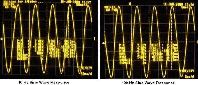
Sine wave 10 Hz and 100 Hz

Sine wave 1 kHz and 10 kHz
100 kHz and 1 MHz signals

Square wave 10 Hz and 100 Hz

Square wave 1 kHz and 10 kHz

60 W total power, 1 kHz symmetry cutoff


Thus, it becomes clear that a simple and high-quality design of an UMZCH is not necessarily made using integrated circuits - only 8 transistors allow you to achieve decent sound with a circuit that can be assembled in half a day.
The amplifier offered to your precious attention is easy to assemble, terribly simple to set up (it actually doesn’t require it), does not contain particularly scarce components, and at the same time has very good characteristics and can easily match the so-called hi-fi, so dearly loved by the majority of citizens .The amplifier can operate at 4 and 8 Ohm loads, can be used in a bridge connection to an 8 Ohm load, and it will deliver 200 W to the load.
Main characteristics:
Supply voltage, V................................................... ............... ±35
Current consumption in silent mode, mA.................................... 100
Input impedance, kOhm................................................... .......... 24
Sensitivity (100 W, 8 Ohm), V............................................ ...... 1.2
Output power (KG=0.04%), W.................................... ........ 80
Reproducible frequency range, Hz.................................... 10 - 30000
Signal-to-noise ratio (not weighted), dB..................... -73
The amplifier is entirely based on discrete elements, without any op-amps or other tricks. When operating at a 4 Ohm load and a 35 V supply, the amplifier develops power up to 100 W. If there is a need to connect an 8 Ohm load, the power can be increased to +/-42 V, in this case, we will get the same 100 W.It is very strongly not recommended to increase the supply voltage above 42 V, otherwise you may be left without output transistors. When operating in bridge mode, an 8-ohm load must be used, otherwise, again, we lose all hope for the survival of the output transistors. By the way, we must take into account that there is no short-circuit protection in the load, so you need to be careful.To use the amplifier in bridge mode, it is necessary to screw the MT input to the output of another amplifier, to the input of which the signal is supplied. The remaining input is connected to the common wire. Resistor R11 is used to set the quiescent current of the output transistors. Capacitor C4 determines the upper limit of the gain and you should not reduce it - you will get self-excitation at high frequencies.
All resistors are 0.25 W except for R18, R12, R13, R16, R17. The first three are 0.5 W, the last two are 5 W each. The HL1 LED is not for beauty, so there is no need to plug a super-bright diode into the circuit and bring it to the front panel. The diode should be the most common green color - this is important, since LEDs of other colors have a different voltage drop.If suddenly someone was unlucky and could not get the output transistors MJL4281 and MJL4302, they can be replaced with MJL21193 and MJL21194, respectively.It is best to take a multi-turn variable resistor R11, although a regular one will do. There is nothing critical here - it’s just more convenient to set the quiescent current.
In this article we will analyze the scheme in detail DIY tube amplifier.
SE or single-ended circuits are amplifiers in which the signal is amplified by one amplifying element (tube, transistor) in series at each stage. These systems operate in pure Class A and are valued by many audiophiles for their good microdynamics and precision in detail presentation. Simplicity is also an advantage. The disadvantages of these circuits are: low energy efficiency (Class A), low gain, slightly higher distortion. We present here a prototype of such an amplifier.
tube amplifier
 Tube amplifier it's not worth it cheap collect. But it is quite possible and realistic collect your own hands. But what to assemble, has been going for more than one year. It is in many ways better than semiconductor ones, and the sound is warmer. And so, let's get started - a diagram and a photo report of a tube amplifier with your own hands with all the files and descriptions.
DIY home theater with lamps
DIY home theater with lamps

For every true audio connoisseur, a tube amplifier speaks volumes, but the latest in fashion is the creation of a complete multi-channel tube home theater. Believe me, with a 32" screen the effect is simply amazing! We use a classic single-ended circuit, with parallel connection of lamps at the output to increase the output power. The amplifier operates in class "A", which ensures maximum sound quality. The lamps can be used for input - 6N1P, 6N2P, 6N23P; for exit - 6P14P, 6P15P, 6P43P, 6P3S - shorter than rich.
Another low purity amplifier on TDA
Do-it-yourself low-frequency amplifier for tda

This amplifier is well suited for assembly and for those who recently began to be interested in radio engineering, have mastered the technology of how to apply tracks to a board and etch it.
The amplifier is assembled on a tda7377 and ne555 microcircuit.
Pout - maximum 20W per channel.
The output power will allow you to enjoy the tracks you like.
DIY low pass filter
Low pass filter for subwoofer circuit
 We all know that a subwoofer low-frequency head without any filters, when connected to a power amplifier, will simply work like a regular speaker, of course reproducing low frequencies perfectly, but without low pass filters You can't build a good subwoofer.
DIY 50W tube amplifier
DIY 50W tube amplifier

Good evening to all fans of radio tube sound! There are a lot of good sound amplifier circuits on the site, so I will publish a mono version of my LUNC. It took me a long time to assemble it, for almost a whole year I periodically took on the project and gradually completed it, and now, finally, the time has come to present the final version for your consideration. Purpose: the usage for the subwoofer channel was calculated.
DIY tube amplifier for guitar
DIY tube amplifier for guitar

Recently there was a need to assemble a simple ULF for guitar, for which the standard was chosen LUNCH scheme using lamps such as 6n23p and 6p14p.
DIY hybrid ULF
DIY hybrid ULF

At numerous requests from radio amateurs, I present an improved and more complete hybrid ULF diagram with a detailed description, parts list and power supply diagram. The lamp at the input of the hybrid ULF 6N6P circuit was replaced with 6N2P. You can also install the 6N23P, which is more common in old lamps, in this unit. Field-effect transistors are replaceable with other similar ones - with an insulated gate and a drain current of 5A and higher.
Variable R1 - 50 kOhm is a high-quality variable resistor for the volume control. You can set it up to 300 kOhm, nothing will worsen. Be sure to check the regulator for the absence of rustles and unpleasant friction during rotation. Ideally, you should use ALPS RG - this is a Japanese company producing high-quality regulators. Don't forget about the balance regulator.
Tube amplifier circuit
DIY lamp unch

Tube amplifiers are becoming increasingly popular among audio lovers. They differ in quality from transistor ones and in a more aesthetically pleasing retro style.
Shown in photo tube ULF not difficult assemble with your own hands.
The author decided to assemble the UMZCH using a push-pull circuit on 6P6S lamps. I’ll say right away that the sound is really not bad, although I haven’t listened to it thoughtfully for a long time. The power is enough for the eyes, although it was difficult to remove the background, especially in the right channel. I assembled it according to the attached diagram, only the rectifier was made on 5TS3S, after the kenatron the capacitor is 47 microfarads, each channel has its own D21 inductor, after each choke there is 330 microfarads of capacitance and it still buzzes a little.
DIY amplifier for K174UN14
DIY amplifier for K174UN14

This amplifier is easy to assemble, UZCH scheme collected on a fairly well-known microcircuit k174un14, which is also an analogue of imported tda2003 chips.
Even beginners in radio engineering can assemble this circuit. And so we look further at the characteristics and the circuit diagram of the device itself sent by Aidar Galimov
Scheme No. 1
Selecting an amplifier class . Let us immediately warn the radio amateur - we will not make a class A amplifier using transistors. The reason is simple - as stated in the introduction, the transistor amplifies not only the useful signal, but also the bias applied to it. Simply put, it amplifies direct current. This current, together with the useful signal, will flow through the acoustic system (AS), and speakers, unfortunately, are able to reproduce this direct current. They do this in the most obvious way - by pushing or pulling the diffuser from its normal position to an unnatural one.
Try to press the speaker cone with your finger - and you will see what a nightmare the sound produced will turn into. Direct current in its action successfully replaces your fingers, so it is absolutely contraindicated for a dynamic head. You can separate direct current from an alternating signal by only two means - a transformer or a capacitor - and both options, as they say, are worse than the other.
Schematic diagram
The circuit of the first amplifier that we will assemble is shown in Fig. 11.18.
This is a feedback amplifier, the output stage of which operates in mode B. The only advantage of this circuit is its simplicity, as well as the uniformity of the output transistors (no special complementary pairs are required). However, it is quite widely used in low-power amplifiers. Another advantage of the scheme is that it does not require any configuration, and if the parts are in good working order, it will work immediately, and this is very important for us now.
Let's consider the operation of this circuit. The amplified signal is supplied to the base of transistor VT1. The signal amplified by this transistor from resistor R4 is supplied to the base of the composite transistor VT2, VT4, and from it to resistor R5.
Transistor VT3 is turned on in emitter follower mode. It amplifies the positive half-waves of the signal on resistor R5 and supplies them through capacitor C4 to the speaker.
The negative half-waves are enhanced by the composite transistor VT2, VT4. In this case, the voltage drop across diode VD1 closes transistor VT3. The signal from the amplifier output is fed to the feedback circuit divider R3, R6, and from it to the emitter of the input transistor VT1. Thus, transistor VT1 plays the role of a comparison device in the feedback circuit.
It amplifies direct current with a gain equal to unity (because the resistance of capacitor C to direct current is theoretically infinite), and the useful signal with a gain equal to the ratio R6/R3.
As you can see, the capacitance value of the capacitor is not taken into account in this formula. The frequency from which the capacitor can be neglected in calculations is called the cutoff frequency of the RC circuit. This frequency can be calculated using the formula
F = 1 / (R×C).
For our example, it will be about 18 Hz, i.e. the amplifier will amplify lower frequencies worse than it could.
Pay . The amplifier is assembled on a board made of single-sided fiberglass 1.5 mm thick with dimensions 45×32.5 mm. The PCB layout in a mirror image and the parts layout can be downloaded. You can download a video about the operation of the amplifier in MOV format for viewing. I want to immediately warn the radio amateur - the sound reproduced by the amplifier was recorded in the video using the microphone built into the camera, so, unfortunately, it will not be entirely appropriate to talk about the sound quality! The appearance of the amplifier is shown in Fig. 11.19.
Element base . When manufacturing an amplifier, transistors VT3, VT4 can be replaced with any transistors designed for a voltage not less than the supply voltage of the amplifier, and a permissible current of at least 2 A. The diode VD1 must also be designed for the same current.
The remaining transistors are any with a permissible voltage of at least the supply voltage, and a permissible current of at least 100 mA. Resistors - any with a permissible power dissipation of at least 0.125 W, capacitors - electrolytic, with a capacitance not less than indicated in the diagram, and an operating voltage less than the supply voltage of the amplifier.
Radiators for amplifier . Before we try to make our second design, let us, dear radio amateur, focus on radiators for the amplifier and present here a very simplified method for calculating them.
First, we calculate the maximum power of the amplifier using the formula:
P = (U × U) / (8 × R), W,
Where U- amplifier supply voltage, V; R- speaker resistance (usually it is 4 or 8 ohms, although there are exceptions).
Secondly, we calculate the power dissipated on the collectors of the transistors using the formula:
P race = 0.25 × P, W.
Thirdly, we calculate the radiator area required to remove the corresponding amount of heat:
S = 20 × P race, cm 2
Fourthly, we select or manufacture a radiator whose surface area will be no less than the calculated one.
This calculation is very approximate, but for amateur radio practice it is usually sufficient. For our amplifier, with a supply voltage of 12 V and an AC resistance of 8 Ohms, the “correct” radiator would be an aluminum plate measuring 2x3 cm and at least 5 mm thick for each transistor. Keep in mind that a thinner plate does not transfer heat well from the transistor to the edges of the plate. I would like to warn you right away - the radiators in all other amplifiers must also be of “normal” sizes. Which ones exactly - count for yourself!
Sound quality . After assembling the circuit, you will find that the sound of the amplifier is not entirely clear.
The reason for this is the “pure” class B mode in the output stage, the characteristic distortions of which even feedback is not able to completely compensate. For the sake of experiment, try replacing transistor VT1 in the circuit with KT3102EM, and transistor VT2 with KT3107L. These transistors have a significantly higher gain than KT315B and KT361B. And you will find that the amp's sound has improved significantly, although some distortion will still be noticeable.
The reason for this is also obvious - a higher gain of the amplifier as a whole ensures greater accuracy of the feedback and a greater compensating effect.
Continue reading
We also recommend
 We connect the pumping station to the well
 Construction level GOST 9416 93
 Appendix II proposals for structural adaptations of columnar and strip foundations to construction conditions on heaving soils
 Concrete columnar foundation
 DIY columnar strip foundation
 How to find a team of builders to build a house - my experience Need a construction team to build a house