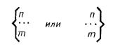
Designation of elements on the diagram according to GOST. General rules for constructing a corner
Download document

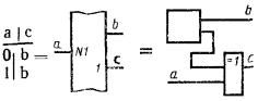
UNIFIED SYSTEM OF DESIGN DOCUMENTATION
CONDITIONAL GRAPHIC DESIGNATIONS IN SCHEMES.
ELEMENTS OF DIGITAL EQUIPMENT
GOST 2.743-91
GOSSTANDART OF RUSSIA
Moscow - 1992
STATE STANDARD OF THE UNION OF THE SSR
1. GENERAL PROVISIONS
1.1. Element of digital technology (hereinafter - element) - a digital or microprocessor microcircuit, its element or component; digital microassembly, its element or component. Definitions of digital and microprocessor microcircuits, their elements and components - according to GOST 17021, definitions of a digital microassembly, its element or component - according to GOST 26975.
Note. The elements of digital technology conditionally include elements that are not intended for converting and processing signals that change according to the law of a discrete function, but are used in logical circuits, for example, a capacitor, a generator, etc.
1.2. When constructing the UGO, the symbols "0" and "1" are used to identify two logical states "logical 0" and "logical 1" (Appendix 1).
2. RULES FOR CONSTRUCTION OF HUGO ELEMENTS
2.1. General rules for constructing UGO
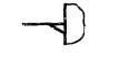
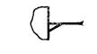
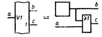
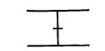
2.1.1. The UGO of the element has the shape of a rectangle, to which the lines of conclusions are brought. The UGO of an element can contain three fields: the main one and two additional ones, which are located to the left and to the right of the main one (Fig. 1).
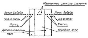
Note. In addition to the main and additional fields of the UGO element, it can also contain a circuit of a common control unit and a circuit of a common output element (Appendix 2).
2.1.2. In the first line of the main field of the UGO, the designation of the function performed by the element is placed. The following lines of the main field contain information according to GOST 2.708.
Note. It is allowed to put information in the main field from the first position of the line, if this does not lead to ambiguity in understanding.
Additional fields contain information about pin assignments (pin labels, pointers).
It is allowed to put down pointers on the output lines on the UGO circuit, as well as between the output line and the UGO circuit.
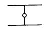
2.1.3. UGO can consist only of the main field (Table 1, item 1) or of the main field and one additional field, which is located to the right (Table 1, item 2) or to the left (Table 1, item 3) of the main one, as well as from the main field and two additional ones (Table 1, item 4).
It is allowed to divide additional fields into zones, which are separated by a horizontal line.
The main and additional fields may not be separated by a line. At the same time, the distance between alphabetic, numeric or alphanumeric designations placed in the main and additional fields is determined by the unambiguous understanding of each designation, and for designations placed on one line, there must be at least two letters (numbers, signs) that make these designations.
Table 1
2. The elements depicted in a combined way are allowed to be separated graphically by communication lines, while the distance between the ends of the UGO contour lines and the communication lines must be at least 1 mm (Fig. 2).
2.1.4. The outputs of the elements are divided into inputs, outputs, bidirectional outputs and outputs that do not carry logical information.
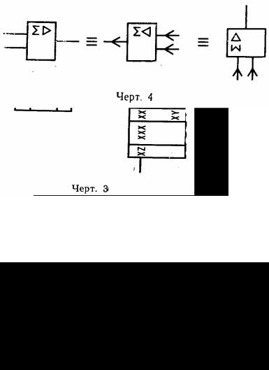
The inputs of the element are depicted on the left side of the UGO, the outputs - with right side UGO. Bidirectional conclusions and conclusions that do not carry logical information are depicted on the right or left side of the UGO.
Note. With UGO orientations, when the inputs are on the right or below, and the outputs are on the left or above, it is necessary to put arrows on the output (connection) lines indicating the direction of information propagation, while the designation of the element function must correspond to that shown in Fig. 4.
2.1.7. The dimensions of the UGO determine:
height:
number of output lines;
number of intervals;
number of lines of information in the main and additional fields, font size;
in width:
the presence of additional fields;
the number of characters placed in one line inside the UGO (including spaces), font size.
2.1.8. The ratios of the sizes of designations of functions, labels and pointers of conclusions in UGO, as well as the distances between the lines of conclusions must correspond to those given in Appendix 5.
The minimum grid step M is selected based on the requirements of microfilming (GOST 13.1.002).
2.1.9. The inscriptions inside the UGO are performed in the main font according to GOST 2.304.
When performing UGO using computer output devices, the fonts available in them are used.
2.2. Element Function Designations
2.2.1. The designation of functions or a set of functions (hereinafter referred to as functions) performed by an element is formed from capital letters of the Latin alphabet, Arabic numerals and special characters written without spaces.
The number of characters in the designation of a function is not limited, however, one should strive for their minimum number while maintaining the unambiguity of understanding of each designation.
2.2.2. The designations of the functions of the elements are given in Table. 2.
table 2
|
Name |
Designation |
|
2. Calculator: |
|
|
calculator section |
|
|
computing device |
|
|
3. Calculator |
P-Q or SUB |
|
4. Divider |
|
|
5. Demodulator |
|
|
6. Demultiplexer |
|
|
7. Decoder |
|
|
8. Discriminator |
|
|
9. Display |
|
|
10. Programmable peripheral interface |
|
|
11. Inverter, repeater |
|
|
12. Comparator |
COMP |
|
13. Microprocessor |
|
|
14, Modulator |
|
|
15. Modifier |
|
|
16. Memory |
|
|
17. Main memory |
|
|
18. Main memory |
|
|
19. Fast memory |
|
|
20. First-in, first-out memory |
|
|
21. Read Only Memory (ROM): |
|
|
programmable ROM (PROM) |
|
|
PROM with the possibility of multiple programming (REPROM) |
|
|
reprogrammable PROM with ultraviolet erasure (RPROM) |
|
|
22. Random Access Memory (RAM): |
|
|
random access RAM static (SRAM) |
|
|
Dynamic Random Access RAM (DRAM) |
|
|
non-volatile RAM (ENOZU) |
|
|
23. Associative storage device |
|
|
24. Programmable Logic Matrix (PLA) |
|
|
25. Converter |
|
|
Notes: 1. Letters X and Y can be imputed by the designations of the information presented at the inputs and outputs of the converter, for example: |
|
|
analog |
|
|
digital |
# or D |
|
binary |
|
|
decimal |
|
|
binary decimal |
|
|
octal |
|
|
hexadecimal |
|
|
seven-segment |
|
|
TTL level |
|
|
MOS level |
|
|
ESL level |
|
|
2. Designations are allowed: |
|
|
digital-to-analogue converter |
|
|
analog to digital converter |
|
|
26. Bus transceiver |
|
|
27. Processor |
|
|
Processor section |
|
|
28. Register |
|
|
shift register n-bit |
|
|
29. Adder |
S or SM |
|
30. Counter: |
|
|
counter n-bit |
|
|
modulo counter n |
|
|
31. Trigger |
|
|
Two stage trigger |
|
|
Note. It is allowed not to specify the function designation when executing UGO triggers |
|
|
32. Multiplier |
n or MPL |
|
33. Amplifier |
|
|
34. Device |
|
|
35. Arithmetic-logical device |
|
|
36. Priority coding device |
|
|
37. Switching device, electronic key |
|
|
BUS or AT |
|
|
39. Encoder |
|
|
40. Delay element |
|
|
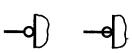
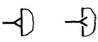
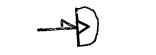
41. Logic element: |
? n or >= n |
|
"majority" |
|
|
"XOR" |
EXOR or = 1 |
|
"logical AND" |
|
|
Note. When performing UGO using computer output devices, it is allowed to designate the function |
|
|
"logical AND" |
|
|
"logical OR" |
|
|
« n only n» |
|
|
"odd" |
2k+ 1 or 2 K + 1 |
|
"parity" |
2k or 2 K |
|
42. Element of mounting logic: |
|
|
"mounting OR" |
|
|
"mounting AND" |
|
|
43. Monostable element, single vibrator: |
|
|
with restart |
|
|
without restart |
|
|
44. Non-logical element: |
|
|
stabilizer, general designation |
|
|
Voltage regulator |
|
|
current stabilizer |
|
|
45. Sets of non-logical elements |
|
|
resistors |
|
|
capacitors |
|
|
inductors |
|
|
diodes with indication of polarity |
|
|
transistors |
|
|
transformers |
|
|
indicators |
according to GOST 2.764 |
|
fuses |
|
|
combined, for example, diode-resistor |
|
|
46. Unstable element, generator: |
|
|
general designation |
|
|
Note. If the waveform is obvious, the designation " G" without "". |
|
|
with synchronized start |
|
|
with stop synchronization at the end of the impulse |
|
|
with synchronized start and stop |
|
|
square wave generator |
|
|
continuous pulse generator |
|
|
ramp generator |
|
|
sine wave generator |
|
|
47. Threshold element, hysteresis |
2.2.3. The sign "*" is put down before the designation of the function of the element, if all its conclusions are non-logical.
2.2.4. It is allowed to add to the function designation on the right specifications element, for example:
47 ohm resistor - * R 47.
The element delay is indicated as shown in Fig. 5.
If the two delays are equal, then only one value of 10 ns is indicated.
Notes
1. The delay, expressed in seconds or in units based on the number of words or bits, can be specified both inside the delay element UGO loop and outside it.
2. It is allowed to specify the delay value as a decimal number:
3 or DEL3, while the value of the delay unit must be specified in the circuit field or in technical requirements
3. In the UGO element, it is allowed to omit a space between the numerical value and the unit of measurement, for example, RAM16K, 10 ns, + 5 V.
2.2.5. If it is necessary to specify a complex function of an element, a composite (combined) designation of the function is allowed.
For example, if an element performs several functions, then the designation of its complex function is formed from several more simple notation functions, while their sequence is determined by the sequence of functions performed by the element:
four-digit counter with a decoder at the output CTR4DC;
Converter/amplifier BCD to seven-segment code BCD/7SEG>.
The designation of a complex function of an element can also be composed of a function designation and an output label explaining this function designation, with the output label preceding the function designation, for example:
fast transfer generator CPG;
data register DRG;
selector (selection device) SELDEV.
2.2.6. When using the designations of the functions of elements that are not established by this standard, they must be explained in the field of the diagram.
2.3. Designation of terminals of elements
2.3.1 The conclusions of the elements are divided into bearing and non-carrying logical information.
Conclusions that carry logical information are divided into static and dynamic, as well as direct and inverse.
2.3.2. On a direct static output, a binary variable has the value "1" if the signal on this output in the active state is in the "logical 1" state (hereinafter referred to as LOG1)
On the inverted static output, the binary variable has the value "1" if the signal on this output in the active state is in the "logical 0" state (hereinafter referred to as LOG0
On a direct dynamic pin, a binary variable has the value "1" if the signal on that pin changes from the state LOG0 into a state LOG1 in the accepted logical convention.
On an inverted dynamic pin, the binary variable has the value "1" if the signal on that pin changes from the state LOG1 into a state LOG0 in the accepted logical convention.
2.3.3 Properties of conclusions in accordance with paragraphs. 2.3.1 and 2.3.2 are indicated by pointers (Table 3)
Table 3
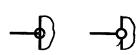
|
Name |
Designation |
|
|
1. Direct static input |
||
|
2. Direct static output |
||
|
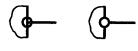
3. Inverse static input |
|
|
|
4. Inverse static output |
|
|
|
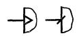
5. Direct dynamic input |
|
|
|
6. Inverse dynamic input |
|
|
|
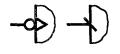
7. Static input with polarity indicator |
|
|
|
8. Static output with polarity indicator |
|
|
|
9. Dynamic input with polarity indicator Note to paragraphs. 7 - 9. Pointers are used when the state LOG1 corresponds to a less positive level. |
|
|
|
10. Conclusion that does not carry logical information: |
||
|
pictured on the left |
|
|
|
pictured on the right |
|
|
Notes:
1. Form 1 is preferred.
2. When performing UGO using computer output devices, it is allowed to perform:
inverse static input, output - letter O;
direct dynamic input - symbol > or /;
inverse dynamic input - symbol< или;
output that does not carry logical information - the letter X.
2.3.4. The pointer of non-logical conclusions is not affixed to the conclusions of the UGO element if the sign “*” of the non-logical element is placed before the designation of its function.
2.3.5. The functional purpose of the pins of the element is indicated by pin labels.
The output label is formed from capital letters of the Latin alphabet, Arabic numerals and (or) special characters written in one line without spaces.
The number of characters in the label is not limited, but should be as small as possible while maintaining the unambiguous understanding of each designation.
The designations of the main labels of the outputs of the elements are given in table. 4.
Table 4
|
Name |
Designation |
|
ADR or A |
|
|
4. Blocking: |
|
|
5. Fault signal blocking |
|
|
6. Input (information) |
|
|
8. Branching |
|
|
9. Recovery |
|
|
10. Two-threshold input, hysteresis input |
|
|
11. Associative storage request input |
|
|
12. Count down input (reduce input) |
- n or DOWN |
|
13. The input of the operand on which one or more mathematical operations are performed |
|
|
Notes: 1. Parameter n is replaced by the decimal equivalent of that bit. If the values of all inputs Рn there are degrees with base 2, n can be replaced by binary order. |
|
|
2. If there is a second operand, its designation is preferably " Q». |
|
|
14. Direct count input (increase input) |
+ P or U.P. |
|
Note to paragraph 12, 14. Parameter n should be replaced by the value by which the contents of the counter are incremented or decremented |
|
|
15. An input that causes the element's output state to change to an additional one each time it takes a state LOG1 |
|
|
16. Digital comparator inputs: |
|
|
17. Choice (selection) |
SEL or SE |
|
18. Address selection: |
|
|
19. Crystal selection, memory access |
|
|
20. Conclusion (of information) |
|
|
21. Output bidirectional |
< >or " |
|
22. The output is free (having no inner connection in the element) |
|
|
23. Fixed mode (status) output |
|
|
24. An output whose state change is delayed until the signal that caused the change returns to its original level. |
|
|
25. Open output (for example, open collector output, open emitter output) |
|
|
26. Exit open H-type(e.g. open collector p-n-r n-p-n transistor, open drain R channel, open source N channel) |
|
|
27. Exit open L-type(e.g. open collector n-p-n transistor, open emitter p-n-p transistor, open source R channel, open drain N channel) |
|
|
28 Three-state output |
|
|
Note. When performing design documentation using a computer output device, the designation is allowed |
|
|
29. Associative storage compare output |
|
|
30. Digital comparator output: |
|
|
* > * or * > |
|
|
* < * или * < |
|
|
*=* or *= |
|
|
Note. The "*" sign must be replaced by operand designations (clause 13) |
|
|
31. Generation |
|
|
32. Ready |
|
|
33. A group of conclusions combined inside an element: |
|
|
34. Grouping bits of a multi-bit input or output |
|
|
Note. n ... m are replaced by decimal equivalents of real significance or binary exponent. Intermediate values between n and m can be omitted |
|
|
35. Grouping links: |
|
|
weekend |
|
|
Note. The designation is used when it is necessary to indicate that several outputs are used to transmit the same information. |
|
|
36. Data: |
|
|
weekend |
|
|
consecutive |
|
|
Note. For storage devices, the following designations are allowed: |
|
|
input information |
|
|
imprint |
|
|
38. Delay |
|
|
39. Delay double |
|
|
entrance accepting a loan |
|
|
loan outlet |
|
|
loan formation |
|
|
loan extension |
|
|
41. Busy |
|
|
42. Write (record command) |
|
|
KEQ or RQ |
|
|
46. Imitation |
|
|
47. Invert (negation) |
|
|
48. Instruction, command |
|
|
49. Acknowledgment |
|
|
51. Switching (electronic) |
|
|
53. Correction |
|
|
54. "logical 0" |
LOGO or LOG0 |
|
55. "logical 1" |
|
|
56. Mask, disguise |
|
|
57. Marker |
|
|
58. Multiplexing |
|
|
59. Odd |
|
|
60. Waiting |
WAIT or wt |
|
61. Operation |
|
|
62. Stop |
|
|
65. Cleaning |
|
|
66. Mistake |
ERR or ER |
|
Error word |
|
|
67. Transfer |
|
|
68. Transfer: |
|
|
input receiving carry |
|
|
carry propagating output |
|
|
transfer formation |
|
|
carry propagation |
|
|
69. Overflow |
|
|
70. Reception confirmation |
|
|
71. Position |
|
|
72. Interruption: |
|
|
interrupt confirmation |
|
|
programmable interrupt |
|
|
74. Priority |
PRI or PR |
|
75. Sequel |
|
|
76. Start, start |
START or ST |
|
77. Work |
|
|
78. Resolution |
|
|
79. Permission for the passage of pulses, the operation of the circuit |
|
|
80. Resolution of the third state |
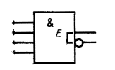
EN or E ? |
|
Note. When performing UGO using computer output devices, the designation is allowed |
|
|
M or MO |
|
|
82. Zero result |
|
|
zeroing |
RES or R |
|
from left to right and from top to bottom (from the least significant digit to the most significant) |
|
|
from right to left or from bottom to top (from the most significant digit to the youngest) |
|
|
Note. Parameter n should be replaced by the actual value of the positions to which the shift occurs. At n= 1 this value can be omitted. |
|
|
left or right |
|
|
85. Synchronization |
SYNC or SYN |
|
86. State |
|
|
87. Medium |
|
|
88. Strobe (sampling signal) |
STR or ST |
|
an input that specifies the content of the element |
|
|
output indicating the contents of the element |
|
|
Note. The "*" sign should be replaced with the value of the element's content |
|
|
90. Reading (reading) |
|
|
CL or CLK |
|
|
92. Management |
|
|
93. Condition |
|
|
94. Set to "1" |
|
|
95. Setting the JK flip-flop: |
|
|
to LOG1 state (J-input) |
|
|
to LOG0 state (K-input) |
|
|
96. Function |
|
|
97. Parity |
2.3.6. The designation of the main labels indicating the functional purpose of the conclusions that do not carry logical information are given in Table. 5.
Table 5
|
Name |
Designation |
|
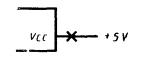
1. Power supply output from the voltage source |
|
|
Notes: |
|
|
1. When performing UGO using computer output devices, the designation is allowed |
|
|
2. Designation allowed |
|
|
3. The supply voltage rating is affixed next to the UGO above the output line or next to it, for example |
|
|
It is allowed to put down the voltage rating inside the UGO instead of the output label, for example |
|
|
4. Before the output label, it is allowed to put down explanatory information, for example: |
|
|
serial number; |
|
|
power indicator of the digital part of the element; |
|
|
analogue part power indicator |
|
|
2. Common terminal, ground, body |
|
|
Notes: |
|
|
1. Designation is allowed. |
|
|
2. Before the output label, it is allowed to put the pointer of the common output of the digital part and the pointer of the common output of the analog part |
|
|
Notes: |
|
|
1. Instead of the designation " I» you can put down its value, for example |
|
|
2. It is allowed to put a serial number before the output label, for example |
|
|
4. Conclusion for connecting a capacitor |
|
|
5. Terminal for connecting a resistor |
|
|
6. Conclusion for connecting inductance |
|
|
7. Conclusion for connecting a quartz resonator |
|
|
8. FET terminals: |
|
|
source |
|
|
9. Conclusions n-p-n and p-n-p transistor: |
|
|
collector |
|
|
emitter n-p-n transistor |
|
|
emitter p-n-p transistor |
|
2.3.7. If it is necessary to specify a complex function of pins, it is allowed to build a composite label formed from the main labels, while it is recommended to follow the reverse order of attaching labels, for example:
read address RDA;
data byte DBY;
byte selection BYSEL.
To indicate an output label that has two functions in turn, these functions are indicated by a slash, for example:
input Output I/O;
write/read WR/RD;
control/data C/D.
Notes:
1. The order of the labels determines the logical level of the enable signal: the first function is performed when LOG1, the second - at LOG0.
2. The order of labels of outputs that do not carry logical information is arbitrary.
3. When performing the UGO of an element that has two ports for receiving and transmitting information: BUT and AT, output label BUT/AT means permission to receive information on the port BUT and information transfer by the port AT at the logic level of the signal at this pin, equal to LOG1.
2.3.8. As pin labels, it is allowed to use the designations of the functions given in Table. 2, for example:
comparison COMP;
the result of a subtraction operation P-Q.
It is also allowed to compose a complex output label from a function designation and an output label, while the direct order of their attachment is recommended, for example:
reading from memory RDM.
2.3.9. When displaying a compound function or output label, it is allowed to execute it in two lines - one under the other, for example:
RAM; DOUT.
2.3.10. If it is necessary to depict a free output in the UGO (having no connections inside the element), then it must have an output pointer that does not carry logical information, and have the output label “ NC».
2.3.11. The power supply outputs of the elements are given either as textual information in the free field of the circuit, or in one of the ways shown in Fig. 6.
|
Power outputs in the common control unit IC DD1 |
Power outlets in one of the elements IC DD2, depicted in an exploded way |
Power pins IC DD3 in a separate loop |
|
|
|
|
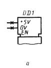
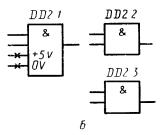
Note. In one set of design documentation, it is allowed to use either the methods shown in Fig. 6 a and 6 b or to hell. 6 a and 6 in.
2.3.12. The numbering of the outputs of the elements is given above their output line to the left for inputs or to the right for outputs from the UGO circuit or the output indicator - if any.
Note. It is allowed to give the numbering of the outputs of the elements in the break of the output line.
2.3.13. When using terminal labels that are not established by this standard, they should be given in the UGO in brackets and explained in the diagram field (Fig. 7) or in the regulatory and technical documentation for the product.
Note. It is allowed to supplement the output label established by this standard with an explanatory output label not specified by this standard, while it is placed in parentheses and, if necessary, explained in the diagram field, for example: EN (P/S) - allow parallel or serial connection of triggers inside the element.
2.4. Designation of output groups
2.4.1. The conclusions of the elements are divided into logically equivalent, i.e. interchangeable without changing the function of the element, and logically unequal.
2.4.2. The UGO element is performed without additional fields or without the right or left additional field, in the following cases:
all conclusions are logically equivalent;
pin functions are uniquely determined by the element function.
In this case, the distances between the pins must be the same, and the labels of the pins are not indicated.
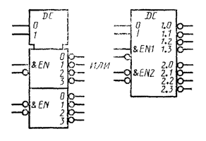
2.4.3. If there are logically equivalent inputs or outputs of an element, they can be graphically combined into a group of outputs, which is assigned a label indicating their function. This label is put down at the level of the first output of the group (Fig. 8).
Note. The numbering of the conclusions of such groups of logically equivalent conclusions may be indicated in any order.
2.4.4. If several consecutive pins have parts of labels that reflect the same functions, then such pins can be combined into a group of pins, and this part of the label is placed in a group label. A group mark is placed above a group of marks, which should be written without line spacing (Fig. 9).
2.4.5. Groups of outputs are separated by an interval of one line or placed in a zone separate for each group.
2.4.6. From several group labels, a group label of a higher order can be extracted. This label is placed above the groups of conclusions to which it belongs, separated from them by an interval.
Groups that belong to a group label of a higher order are placed in a separate zone (Fig. 10).
Note. It is allowed to omit a space between groups of pins that have a label of a higher order.
2.4.7. The numbers of digits in the groups of conclusions are indicated by the numbers of the natural series, starting from zero. In this case, the labels of the conclusions are assigned by one of the methods presented in Fig. eleven.
Note. For outputs, pin labels are allowed, consisting only of digit numbers. Only open and tri-state exit labels are required.
If weight coefficients are uniquely defined in a group of digits, then instead of the digit number, its weight coefficient can be affixed. For example, for binary reckoning, a series of weights looks like 2 0 , 2 1 , 2 2 , 2 3 , ... = 1, 2, 4, 8, ... D1 or 1 , the third category - D8 or 8 .
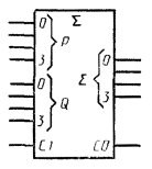
2.4.8. If it is necessary to number the groups and digits within the group, the label of each output will consist of the group number (first digit) and the digit number in the group, separated from each other by a dot, for example: the label of the information input of the first digit of the zero group: D 0.1.
Note. If there are two information channels (ports) in the element, their designation is allowed BUT and AT, which are taken out as a group label for information inputs and (or) outputs, if this does not lead to an ambiguous understanding of output labels.
2.4.9. Bidirectional output is indicated by the label "< >” or ““”, which is put down either in the UGO of the element - above or next to the function label (group function label) of the output (outputs) - hell. 12 a and hell. 12 b respectively, or on the terminals of the element (Fig. 12 in). In this case, the labels of the pins denoting the input and output functions are put through a slash.
Note. It is allowed to put labels of input and output output functions above and below the bidirectional output label, respectively (Fig. 12 G).
![]()
2.5. Relationship of conclusions
2.5.1. The conclusions of the elements are divided into influencing and dependent. An influencing pin affects one or more dependent pins.
2.5.2. To indicate the relationship of the conclusions of the element, the dependency designation is used.
The designation of the dependence of pins is carried out by assigning pin labels to them:
for the influencing conclusion - the letter designation of the dependency in accordance with Appendix 3 and the serial number affixed after the letter designation without a space;
for each dependent on this influencing output - the same serial number, affixed without a space before the letter designation of the output label assigned to it in accordance with Table. 4, or instead.
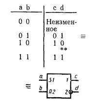
If the influencing output affects the dependent output with its additional logical state, then a dash is placed above the serial number before the label of the dependent output (Fig. 13 a).
If the conclusion is dependent on several influencing conclusions, the serial number of each of them must be indicated separated by commas (Fig. 13 b).
Note. It is allowed to supplement the dependency designation with a label explaining the functional purpose of the output, which is placed in parentheses.
2.5.3. If the output performs several functions and (or) has several influencing influences, then the designation of each of these functions and (or) dependencies by the corresponding label can be shown either in subsequent lines, while each label can be assigned a pointer (Fig. 14 a), or on one line through a slash (Fig. 14 b). The order of labels denoting multiple functions or dependencies is arbitrary.
Note. When specifying several labels of one conclusion in subsequent lines, it is allowed not to draw lines of conclusions to them.
3. DESIGNATION OF INSTALLATION LOGIC
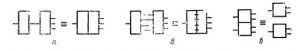
3.1. The direct connection of the logical outputs of several elements to a common load (wiring logic) should be designated as shown in Fig. fifteen a.
3.2. Mounting logic can be considered conditionally as an element that is depicted as a UGO element of mounting logic (Fig. 15 b).
Notes to paragraphs. 3.1, 3.2:
1. The term "wiring logic element" corresponds to the term "DOT element".
2. Depending on the type of logical function being performed, the “*” sign should be replaced by the “&” sign (“wiring AND”) or the “1” sign (“wiring OR”).
3. It is allowed to depict the installation logic, as shown in Fig. fifteen in, if it does not lead to ambiguity of understanding.
4. If the outputs of the elements are assigned labels of open outputs, it is allowed to depict the installation logic in accordance with Fig. fifteen G.
4. ABBREVIATED DESIGNATION OF UGO GROUPS
4.1. To reduce the volume of documentation, the abbreviated designation of UGO groups is allowed.
4.2. UGO elements can be depicted combined, adjacent to each other by one or two sides parallel to the distribution of information (Fig. 16 a). There is no logical connection between these elements.
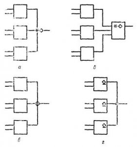
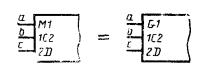
Note. It is allowed to depict UGO elements with a common side perpendicular to the dissemination of information (Fig. 16 b). In this case, there is at least one logical connection between these elements. Logical connections should be indicated in accordance with Appendix 4. In the absence of such instructions, it is considered that there is only one logical connection between these elements (Fig. 16 in).
4.3. UGO of a group of elements of the same type, depicted in combination and having the same information and common conclusions, may contain a common graphic block - a control block (Appendix 3). It is allowed to designate the control unit as shown in Fig. 17.
4.4. In a group of elements depicted combined and containing the same information in the main UGO field, the latter is placed in the upper UGO (Fig. 18 a). It is allowed to separate such elements from each other with a dashed line (Fig. 18 b).
Two consecutive groups of elements should be depicted as shown in Fig. eighteen in. The abbreviated designation of a group of pairs of elements is shown in Fig. eighteen G.
A group of elements with identical outputs (inputs and outputs), having a common control unit and not having it, is allowed to be depicted as shown in Fig. eighteen d and hell. eighteen G respectively.
4.5. In circuits that have elements with a large number conclusions of one functional purpose, the abbreviated designation of such elements is allowed (Fig. 19).
|
Output number |
||||||||||
|
output label |
||||||||||
|
Output number |
||||||||||
|
output label |
||||||||||
Notes:
1. The records of conclusions 13 - 17 and 13 ... 17 are identical.
2. The table (the first way of abbreviated designation of elements) should be placed on the field of the scheme.
4.6. In schemes with repeating elements, it is also allowed to use the batch method of information compression, i.e. batch image of UGO elements and their connection lines.
4.6.1. A package of elements is a group of elements of the same type, depicted as one UGO. A package of signals is a group of signals (logical connections of elements) depicted by a single line. Packages of elements and signals are explained in the diagram using information packages,
4.6.2. An information package is a short listing of the following data:
signal identifiers (logical connections of elements);
constructive addresses of elements and signals;
coordinates of elements on the scheme;
the number of elements or signals in the packet, etc.
4.6.3. A brief record of the information package can be represented as follows:
0.1; 0.1; 0.1; 0.1 = (0.1) 4 - the sequence 0.1 is repeated 4 times;
0, 0, 0, 1, 1, 1 = 3 (0,1) - each element of the specified sequence is repeated 3 times in a row.
4.6.4. A batch image of information is used when the following conditions are met simultaneously:
uniformity of elements in a group;
uniformity of input and output signals of group elements;
regularity of signals in each packet, allowing their convenient enumeration.
4.6.5. Inside the main field of the UGO package of elements is placed:
in the first three lines, information - according to GOST 2.708;
in subsequent lines, information about the package.
If there is not enough space in the main field, information about the package of elements can be placed in the field of the scheme. For example, to the right of the UGO pack of elements.
An example of a UGO package of elements is shown in Fig. 20.
5. EXAMPLES OF HUGO ELEMENTS
5.1. Examples of UGO elements are given in table. 6 - 15 for the positive logic convention. The given letter designations of functions and pin labels of elements are mandatory, with the exception of the alternative ones given in Table. 2 or in table. 4 (in parentheses). In this case, it is allowed not to indicate serial numbers in pin labels when denoting dependencies.
The order of pin labels (groups of pin labels - if any) is recommended.
The pointers of the conclusions of the elements are given in the preferred form 1 table. 3, however, it is allowed to use all forms of the pointers given in Table. 3.
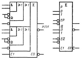
5.2. Examples of UGO logic elements are given in Table. 6.
Table 6
|
Name |
Designation |
|
1. Element "NO" |
|
|
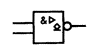
2. Element 3I-NOT |
|
|
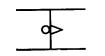
3. Element 2I-NOT with an open collector output and increased load capacity |
|
|
4. Element 3OR-NO |
|
|
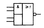
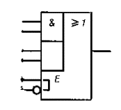
5. Combined 2I-OR element with inverted output |
|
|
6. Element 4I-NO with an open collector at the output |
|
|
7. 2I-OR element with inverted output and expansion input |
|
|
8. Expander |
|
|
9. Even or odd element |
|
5.3. Examples of UGO transceiver elements are given in table. 7.
Table 7
5.4. Examples of UGO hysteresis elements are given in Table. eight.
Table 8
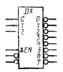
5.5. Examples of UGO converters (decoders) and encoders (encoders) are given in Table. nine.
Table 9
|
Name |
Designation |
|
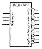
1. BCD to Decimal Code Converter |
|
|
2. Converter from three lines to eight |
|
|
3. Binary to BCD Converter |
|
|
4. Converter-amplifier of binary code to seven-segment. Note. It is allowed to replace lower case uppercase: BUT, AT, With, D, E, F, G |
|
|
5. Priority encoder (priority encoder) from 8 lines to 3 lines (GS- "group signal") |
|
|
6. Two decoders accepting a two-digit code. Note. Designation of decoders is allowed BUT and AT, which are displayed as a group label of the outputs of the corresponding decoder |
|
|
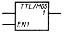
7. Level converter TTL into levels MOS |
|
|
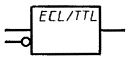
8. Level converter ESL into levels TTL. Note to paragraphs. 7 and 8. The designation of the function of the signal converter */* can be replaced by the designation *//*, if it is necessary to indicate the presence of a galvanic connection between its inputs and outputs |
|
5.6. Examples of UGO multiplexers and demultiplexers, as well as switches for digital and analog signals are given in Table. ten.
Table 10
|
Name |
Designation |
|
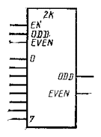
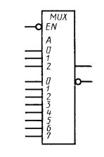
1. Multiplexer for 8 inputs with strobing. Note. Gating input EN allowed to designate STR |
|
|
2. Demultiplexer for 8 lines |
|
|
3. Four-channel multiplexer, two inputs each |
|
|
4. Two-channel multiplexer with 4 inputs each. Note to paragraphs. 3, 4. When designating multiplexer channels not by serial numbers (1, 3, etc.), but by letters BUT, AT etc.) to disambiguate understanding, the data address input is labeled "Select": SEL or SE |
|
|
5. Electronic switch |
|
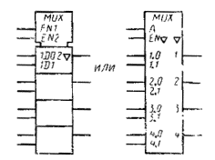
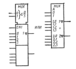
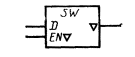
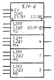
5.7. Examples of UGO arithmetic elements are given in Table. eleven.
Table 11
|
Name |
Designation |
|
1. Full single bit adder |
|
|
2. Four-bit adder-subtractor |
|
|
3. Full adder for 4 bits |
|
|
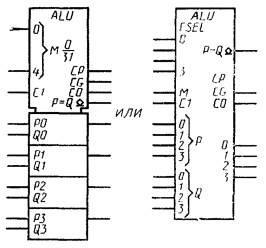
4. Four-digit speed ALU |
|
|
5. Fast transfer generator for ALU |
|
|
6. Four-digit digital comparator |
|
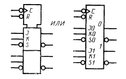
5.8. Examples of UGO triggers (bistable elements) are given in Table. 12.
Table 12
|
Name |
Designation |
|
1. Two triggers with separate launch ( RS-type), one with additional input |
|
|
2. Two delay triggers D-type |
|
|
3. Six D- triggers with common control and reset inputs |
|
|
4. Trigger D-type, triggered on the front |
|
|
5. Trigger JK-type, triggered on the front |
|
|
6. Universal JK-trigger with "master-assistant" structure |
|
|
7. Two JK-trigger with common control and reset inputs |
|
5.9. Examples of UGO monostable (multivibrators) and unstable elements are given in table. thirteen.
Table 13
|
Name |
Designation |
|
1. Standby multivibrator with restart |
|
|
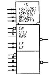
2. Two voltage controlled generators with power leads (LOG- power supply of the digital part of the element, OSC- power supply for the analog part of the element, FC- frequency control) |
|
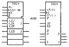
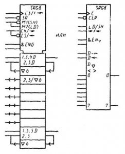
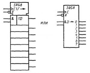
5.10. Examples of UGO registers and counters are given in Table. fourteen.
Table 14
|
Name |
Designation |
|
1. 4-bit shift register with parallel inputs |
|
|
2. Shift 4-bit serial-parallel register with direct and additional code at the output ( T/With- code switching input at the outputs: direct or additional; P/S- input that controls the connection of bits of registers in series or in parallel) |
|
|
3. Shift 4-bit bidirectional universal register |
|
|
4. Universal 8-bit register |
|
|
5. 8-bit shift register with dual serial input and parallel outputs |
|
|
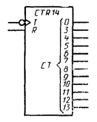
8. Binary 14-bit carry-through counter |
|
|
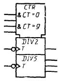
9. Asynchronous decimal counter, consisting of divisors by 2 and 5 with parallel writing |
|
|
10. 4-digit asynchronous decimal counter, consisting of divisors by 2 and by 5 with preset and synchronous reset |
|
5.12. Ratios of the sizes of the main conditional graphic symbols on the modular grid are given in Appendix 5.
LOGICAL AGREEMENT
1. Binary logic deals with variables that can take on two logical states - states "logical 1" (hereinafter - LOG1) and the state "logical 0" (hereinafter - LOG0).
The logical function symbols defined by this standard represent the relationship between the inputs and outputs of elements in terms of logical states not related to the physical implementation.
2. With a specific physical implementation of the elements, the logical states are represented by physical quantities ( electric potential, pressure, luminous flux, etc.). In logic, knowledge of the absolute value of the quantity is not required, so the physical quantity is identified simply as more positive - H and less positive L(Fig. 21). These two values are called logical levels.
3. Correspondence between these concepts is established by the following agreements:
Positive logic convention
More positive meaning physical quantity(logical level H) corresponds LOG1. Less positive value of a physical quantity (logical level L) corresponds LOG0.
Negative logic convention
Less positive value of a physical quantity (logical level L) corresponds LOG1. A more positive value of the physical quantity (logical level H) corresponds LOG0.
4. To indicate the correspondence between logical states and the values of these states, two methods are used:
single agreement method for the entire circuit (positive logic agreement or negative logic agreement);
using a polarity indicator.
5. To establish a one-to-one correspondence between the logical state and the logical level on the output of the element, use the inversion indicator (0) or the polarity indicator ( or ).
6. The inversion indicator is used if a single agreement has been adopted for the entire scheme (as in Fig. 21),
If positive and negative logic conventions are used in the circuit, the polarity indicator of the pins for which the negative logic convention is valid should be used.
In a circuit with polarity indicators, the inversion indicator is not used.
7. On the field of the scheme or in the technical requirements, it must be indicated in which logic the scheme is made.
8. Logical elements may have logical equivalent forms. For example, an element that has a truth table expressed in signal levels, which is shown in Fig. 22 a, has equivalent forms in positive logic and in negative logic, represented in hell. 22 b and hell. 22 in respectively.
|
|
|||
|
|
|||
|
|
|||
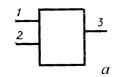
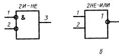
Table 16
CONTOUR DESIGNATIONS
Notes:
1. The ratio of the length of the circuits to their width is not set and is determined by the information placed in the circuit and the number of pins.
2. It is allowed to indicate a common output element in the circuit of a common control unit (for example, output “ST-9” of the UGO counter, table 14, item 12).
Examples of UGO with control loops and a common output element are shown in Fig. 23 a and hell. 23 b respectively.
 EN
EN
Action allowed
Dependent output action disabled: High impedance (HI) external state is set to an open circuit or tri-state output: level L (H) VI is assigned to an output with an open circuit of the type H (L), the rest of the outputs are set to the state LOG 0
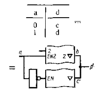
Action allowed
State is set LOG 0
![]()
Action allowed (mode selected)
Action blocked
NEGATION
Additional internal state
Internal state unchanged
SET TO "0"
S = 0,
SET IN "1"
The internal state of the output, as in S = 1,
Internal state unchanged
State is set LOG 1
Action allowed
INTERCONNECTION
State is set LOG 1
State is set LOG 0
* This column shows the state of the influencing output.
** Pseudo-stable condition.
Table 18
INTERNAL CONNECTIONS *
|
Name |
Designation |
|
1. Inner join(internal state LOG1 (LOG0) the input of the right element corresponds to the internal state LOG1 (LOG0) the output of the left element) |
|
|
internal state LOG1 (LOG0) of the right element matches the inner join LOG0 (LOG1) of the output of the left element). Note. The vertical line may cross the "0" inversion indicator. |
|
|
3. Internal connection with dynamic response (internal state LOG1 the input of the right element appears only when the transition of the output of the left element from LOG0 in LOG1, in all other cases, the internal state of the input of the right element is LOG0) |
|
|
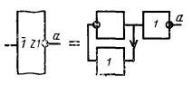
4. Negative inner join with dynamic response |
|
|
5. Internal (virtual) input ( given input is in a state LOG1, if it is not changed by an input with a predominant or modifying dependence, the designation of which is displayed to the right of the first input in accordance with Table. 17. |
|
|
6. Internal (virtual) output (the effect of this output on the internal input to which it is connected is determined by the type of dependence in accordance with Table 17, the designation of which is displayed to the right of this output) Notes to paragraphs. 5 and 6: 1. Internal (virtual) inputs and outputs have only one internal logical state. 2. For internal (virtual) inputs and outputs, only the pin indicators listed in Table 1 apply. 3, paragraph 5 of this standard. |
* An internal connection is a connection within an element (internal inputs and outputs).
Table 19
The size ratios of the UGO on a modular grid are given in Table. nineteen.
|
Name |
Designation |
|
1. Minimum distance between lead lines |
|
|
2. Common control box |
|
|
3. Common output element |
|
|
4. Polarity indicator, e.g. static input with polarity indicator |
|
|
5. Inverted output pointer, such as inverted static input |
|
|
6. Dynamic output pointer, such as inverted dynamic input |
|
|
7. An output pointer that does not carry logical information, such as the one shown on the left |
|
|
8. Bidirectional output label, for example: |
|
|
shown from the entrance |
|
|
shown with polarity indicator |
|
|
9. An exit label whose state change is delayed until the signal that caused the change returns to its original level. V.Yu. Gulenkov, Ph.D. tech. sciences; S.S. Borushek, L.G. Yurganova, V.V. Gugnina |
The UGO of the element has the shape of a rectangle, to which the lines of conclusions are brought. The UGO element can contain three fields: the main one and two additional ones, which are located to the right of the main one (Figure 4).
Figure 4
Note. In addition to the main and additional fields of the UGO element, it can also contain the contour of a common control unit and the contour of a common output element.
In the first line of the main field of the UGO, the designation of the function performed by the element is placed. The following lines of the main field contain information in accordance with GOST 2.708. Additional fields contain information about pin assignments (pin labels, pointers). It is allowed to put down pointers on the output lines on the UGO circuit, as well as between the output line and the UGO circuit.
UGO can consist only of the main field (table 26, item 1) or of the main field and one additional field, which is located to the right (table 26, item 2) or to the left (table 26, item 3) of the main one, as well as from the main field and two additional ones (table 26, p. 4). It is allowed to divide additional fields into zones, which are separated by a horizontal line.
The main and additional fields may not be separated by a line. At the same time, the distance between alphabetic, numeric or alphanumeric designations placed in the main and additional fields is determined by the unambiguous understanding of each designation, and for designations placed on one line, there must be at least two letters (numbers, signs) that make these designations.
Table 26
Notes
1 The signs "*" denote the functions and labels of the outputs of the elements.
2 It is allowed to separate the elements depicted in a combined way by graphic communication lines, while the distance between the ends of the UGO contour lines and the communication lines must be at least 1 mm (Figure 5).
Figure 5
The outputs of the elements are divided into inputs, outputs, bidirectional outputs and outputs that do not carry logical information. The inputs of the element are depicted on the left side of the UGO, the outputs are on the right side of the UGO. Bidirectional conclusions and conclusions that do not carry logical information are depicted on the right or left side of the UGO.
When summarizing the lines of conclusions to the UGO contour, it is not allowed:
Draw them at the level of the sides of the rectangle;
· put arrows on them near the UGO contour, indicating the direction of information.
Another orientation of the UGO is allowed, in which the inputs are located on top, the outputs are on the bottom (Figure 6).
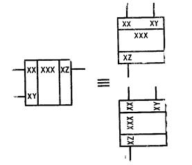
Figure 6
Note - With UGO orientations, when the inputs are on the right or below, and the outputs are on the left or above, it is necessary to put arrows on the output (connection) lines indicating the direction of information propagation, while the designation of the element function must correspond to that shown in Figure 7.
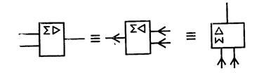
Figure 7
The dimensions of the UGO determine:
a) Height:
The number of output lines
The number of intervals
number of lines of information in the main and additional fields, font size;
b) in width:
the presence of additional fields,
number of characters placed in one line inside the UGO (including spaces), font size.
The ratios of the sizes of function designations, labels and pointers of outputs in the UGO, as well as the distances between the output lines, must correspond to those given in Table 26.
The inscriptions inside the UGO are performed in the main font according to GOST 2.304. When performing UGO using computer output devices, the fonts available in them are used.
Unified system of design documentation
CONDITIONAL GRAPHIC DESIGNATIONS IN SCHEMES. ELEMENTS OF DIGITAL EQUIPMENT
GOST 2.743-91
Introduction date 01.01.93
This International Standard specifies general rules construction of conditional graphic symbols (UGO) of elements of digital technology in schemes performed manually or with the help of printing and graphic output devices of computers in all industries.
1. GENERAL PROVISIONS
1.1. Element of digital technology (hereinafter - element) - a digital or microprocessor microcircuit, its element or component; digital microassembly, its element or component. Definitions of digital and microprocessor microcircuits, their elements and components - in accordance with GOST 17021, definitions of a digital microassembly, its element or component - in accordance with GOST 26975.
Note. The elements of digital technology conditionally include elements that are not intended for converting and processing signals that change according to the law of a discrete function, but are used in logical circuits, for example, a capacitor, a generator, etc.
1.2. When constructing the UGO, the symbols "0" and "1" are used to identify two logical states "logical 0" and "logical 1" (Appendix 1).
2. RULES FOR CONSTRUCTION OF HUGO ELEMENTS
2.1. General rules for constructing UGO 2.1.1. The UGO of the element has the shape of a rectangle, to which lines are drawn
conclusions. The UGO of an element can contain three fields: the main one and two additional ones, which are located to the left and to the right of the main one (Fig. 1).
Note. In addition to the main and additional fields of the UGO element, it can also contain a circuit of a common control unit and a circuit of a common output element (Appendix 2).
2.1.2. In the first line of the main field of the UGO, the designation of the function performed by the element is placed. The following lines of the main field contain information in accordance with GOST 2.708.
Note. It is allowed to put information in the main field from the first position of the line, if this does not lead to ambiguity in understanding.
Additional fields contain information about pin assignments (pin labels, pointers).
It is allowed to put down pointers on the output lines on the UGO circuit, as well as between the output line and the UGO circuit.
2.1.3. UGO can consist only of the main field (Table 1, item 1) or of the main field and one additional field, which is located to the right (Table 1, item 2) or to the left (Table 1, item 3) of the main one, as well as from the main field and two additional ones (Table 1, item 4).
It is allowed to divide additional fields into zones, which are separated by a horizontal line.
The main and additional fields may not be separated by a line. At the same time, the distance between alphabetic, numeric or alphanumeric designations placed in the main and additional fields is determined by the uniqueness of the understanding of each designation, and for designations placed on one line, there must be at least two letters (numbers, signs) that make these designations.
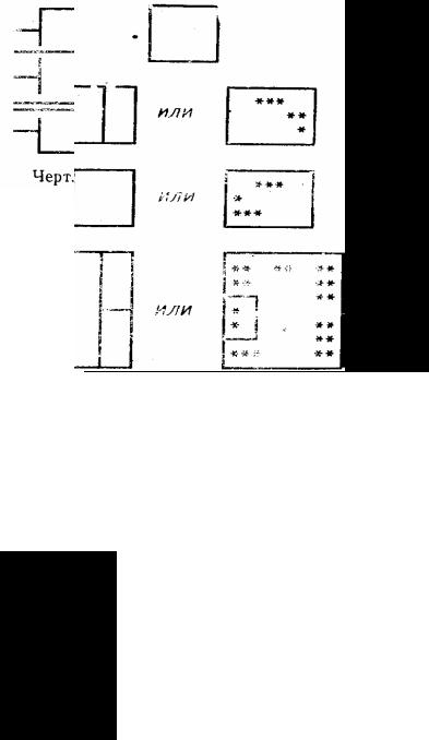
Table 1
Name | Designation |
|
and one (right) additional field | ||
but the (left) extra field | ||
additional, divided into | ||
The number of zones is not limited. | ||
Notes:
1. Signs "*" designate functions and pin labels of elements.
2. It is allowed to separate the elements depicted in a combined way graphically by communication lines, while the distance between the ends of the UGO contour lines and the communication lines must be at least 1 mm (Fig. 2).
2.1.4. The outputs of the elements are divided into inputs, outputs, bidirectional outputs and outputs that do not carry logical information.
The inputs of the element are depicted on the left side of the UGO, the outputs are on the right side of the UGO. Bidirectional conclusions and conclusions that do not carry logical information are depicted on the right or left side of the UGO.
2.1.5. When summing up the lines of conclusions to the contour of the UGO, it is not allowed; draw them at the level of the sides of the rectangle; put arrows on them at the UGO contour indicating the direction of the information
2.1.6. Another orientation of the UGO is allowed, in which the inputs are located on top, the outputs are on the bottom (Fig. 3).
Note. With UGO orientations, when the inputs are on the right or below, and the outputs are on the left or above, it is necessary to put arrows on the output (connection) lines indicating the direction of information propagation, while the designation of the element function must correspond to that shown in Fig. 4.
2.1.7. The dimensions of the UGO are determined: by height:
number of lead lines, number of intervals,
number of lines of information in the main and additional fields, font size;
in width:
the presence of additional fields, the number of characters placed in one line inside the UGO (including spaces), font size.
2.1.8. The ratios of the sizes of designations of functions, labels and pointers of conclusions in UGO, as well as the distances between the lines of conclusions must correspond to those given in Appendix 5.
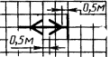
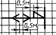
The minimum grid step M is selected based on the requirements of microfilming (GOST 13.1.002).
2.1.9. The inscriptions inside the UGO are performed in the main font according to GOST 2.304. When performing UGO using computer output devices, a font is used
you available in them.
2.2. Element Function Designations
2.2.1. The designation of functions or a set of functions (hereinafter referred to as functions) performed by an element is formed from capital letters of the Latin alphabet, Arabic numerals and special characters written without spaces.
The number of characters in the designation of a function is not limited, however, one should strive for their minimum number while maintaining the unambiguity of understanding of each designation.
2.2.2. The designations of the functions of the elements are given in Table. 2.
table 2
Name | Designation |
|
Calculator: | ||
calculator section | ||
computing device | ||
Calculator | ||
Divider | ||
Demodulator | ||
Demultiplexer | ||
Decoder | ||
Discriminator | ||
10. Peripheral software interface | ||
mimicable | ||
Continuation of the table. 2 |
||
Name | Designation |
|
inverter, repeater | ||
comparator | ||
Microprocessor | ||
Modulator | ||
Modifier | ||
Main memory | ||
main memory | ||
Fast memory | ||
First-in, first-out memory | ||
21. Read Only Memory | ||
programmable ROM (PROM) |
||
PROM with the possibility of multiple | ||
programming (REPZU) | ||
reprogrammable PROM with ultraviolet |
||
flight erasure (RFPZU) | ||
Random Access Memory |
||
random access memory (RAM): | ||
RAM with random access static |
||
skoe (SOZU) | ||
Random Access RAM |
||
cal (DOZU) | ||
non-volatile RAM (ENOZU) |
||
Associative storage device | ||
24. Programmable logic matrix |
||
Converter |
||
Notes: | ||
1. The letters X and Y can be replaced | ||
designations of the presented information | ||
mation at the inputs and outputs of the converter | ||
developer, for example: | ||
analog | I or Λ , or A |
|
digital | ||
binary | ||
decimal | ||
binary decimal | ||
octal | ||
hexadecimal | ||
Continuation of the table. 2
Gray code 7-segment level TTL level MOS level ECL level
2. Designations are allowed: digital-to-analog converter analog-to-digital converter
26. Transceiver tire
27. Processor
Processor section 28. Register
Shift register n-bit
29. Adder
30. Counter: counter n-bit counter modulo n
31. Trigger Two stage trigger
Note. It is allowed not to specify the function designation when executing UGO triggers
32. Multiplier
33. Amplifier
34. Device
35. Arithmetic device
36. Priority coding device
37. Switching device, electronic key
38. Tire
39. Encoder
40. Delay element
GRAY 7SEG TTL MOS ECL
∑ or SM
π or MPL
> or
Continuation of the table. 2 |
||||||||||||||||||||||||||||||||||||||||||||||||||||||||||||||||||||||||||||||||||||||||
Name | Designation |
|||||||||||||||||||||||||||||||||||||||||||||||||||||||||||||||||||||||||||||||||||||||
41. Element | logical: | ≥n or >=n |
||||||||||||||||||||||||||||||||||||||||||||||||||||||||||||||||||||||||||||||||||||||
"majority | ≥ n/2 |
|||||||||||||||||||||||||||||||||||||||||||||||||||||||||||||||||||||||||||||||||||||||
"XOR" | ||||||||||||||||||||||||||||||||||||||||||||||||||||||||||||||||||||||||||||||||||||||||
"logical AND" | ||||||||||||||||||||||||||||||||||||||||||||||||||||||||||||||||||||||||||||||||||||||||
Note. When performing UGO with | ||||||||||||||||||||||||||||||||||||||||||||||||||||||||||||||||||||||||||||||||||||||||
using computer output devices | ||||||||||||||||||||||||||||||||||||||||||||||||||||||||||||||||||||||||||||||||||||||||
the designation of the function “logical | ||||||||||||||||||||||||||||||||||||||||||||||||||||||||||||||||||||||||||||||||||||||||
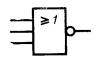
"logical OR" | ≥ 1 or 1 |
|||||||||||||||||||||||||||||||||||||||||||||||||||||||||||||||||||||||||||||||||||||||
"n and only n" | ||||||||||||||||||||||||||||||||||||||||||||||||||||||||||||||||||||||||||||||||||||||||
"odd" | 2k+1 or 2k+1 |
|||||||||||||||||||||||||||||||||||||||||||||||||||||||||||||||||||||||||||||||||||||||
"parity" | ||||||||||||||||||||||||||||||||||||||||||||||||||||||||||||||||||||||||||||||||||||||||
42. Element of mounting logic: | ||||||||||||||||||||||||||||||||||||||||||||||||||||||||||||||||||||||||||||||||||||||||
"mounting OR" | ||||||||||||||||||||||||||||||||||||||||||||||||||||||||||||||||||||||||||||||||||||||||
"mounting AND" | ||||||||||||||||||||||||||||||||||||||||||||||||||||||||||||||||||||||||||||||||||||||||
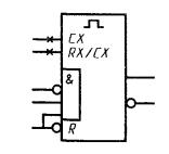
43. The element is monostable, one vib- | ||||||||||||||||||||||||||||||||||||||||||||||||||||||||||||||||||||||||||||||||||||||||
with restart | ||||||||||||||||||||||||||||||||||||||||||||||||||||||||||||||||||||||||||||||||||||||||
without restart | ||||||||||||||||||||||||||||||||||||||||||||||||||||||||||||||||||||||||||||||||||||||||
44. Non-logical element: | ||||||||||||||||||||||||||||||||||||||||||||||||||||||||||||||||||||||||||||||||||||||||
stabilizer, general designation | ||||||||||||||||||||||||||||||||||||||||||||||||||||||||||||||||||||||||||||||||||||||||
Voltage regulator | ||||||||||||||||||||||||||||||||||||||||||||||||||||||||||||||||||||||||||||||||||||||||
current stabilizer | ||||||||||||||||||||||||||||||||||||||||||||||||||||||||||||||||||||||||||||||||||||||||
45. Sets of non-logical elements | ||||||||||||||||||||||||||||||||||||||||||||||||||||||||||||||||||||||||||||||||||||||||
resistors | ||||||||||||||||||||||||||||||||||||||||||||||||||||||||||||||||||||||||||||||||||||||||
capacitors | ||||||||||||||||||||||||||||||||||||||||||||||||||||||||||||||||||||||||||||||||||||||||
inductors | ||||||||||||||||||||||||||||||||||||||||||||||||||||||||||||||||||||||||||||||||||||||||
diodes with indication of polarity | *D → or *D>; *D← or *D< |
|||||||||||||||||||||||||||||||||||||||||||||||||||||||||||||||||||||||||||||||||||||||
transistors | ||||||||||||||||||||||||||||||||||||||||||||||||||||||||||||||||||||||||||||||||||||||||
transformers | ||||||||||||||||||||||||||||||||||||||||||||||||||||||||||||||||||||||||||||||||||||||||
indicators | according to GOST 2.764 |
|||||||||||||||||||||||||||||||||||||||||||||||||||||||||||||||||||||||||||||||||||||||
fuses | ||||||||||||||||||||||||||||||||||||||||||||||||||||||||||||||||||||||||||||||||||||||||
combined, for example, diode- | ||||||||||||||||||||||||||||||||||||||||||||||||||||||||||||||||||||||||||||||||||||||||
resistor | ||||||||||||||||||||||||||||||||||||||||||||||||||||||||||||||||||||||||||||||||||||||||
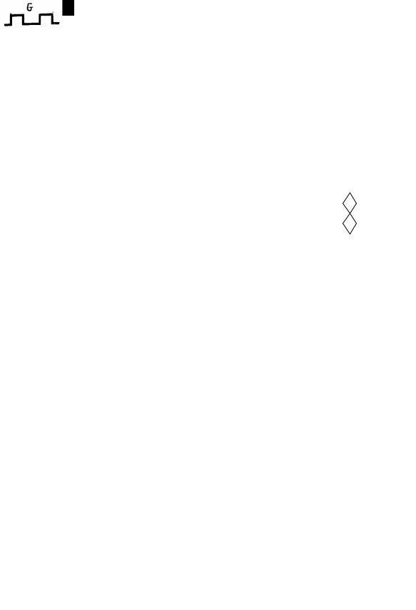
46. Unstable element, generator: | ||||||||||||||||||||||||||||||||||||||||||||||||||||||||||||||||||||||||||||||||||||||||
general designation | ||||||||||||||||||||||||||||||||||||||||||||||||||||||||||||||||||||||||||||||||||||||||
Note. If the waveform is very
2.2.3. The sign "*" is put down before the designation of the function of the element, if all its conclusions are non-logical. 2.2.4. It is allowed to add the technical characteristics of the element to the function designation on the right, for example: 47 ohm resistor - * R 47. The element delay is indicated as shown in Fig. 5.
If these two delays are equal, then only one value is indicated: Notes: 1. The delay, expressed in seconds or in units based on the number of words or bits, can be specified both inside the delay element UGO loop and outside it. 2. It is allowed to specify the delay value as a decimal number. or DEL3, while the value of the delay unit must be specified in the circuit field or in the technical requirements. 3. In the UGO element, it is allowed to omit a space between the numerical value and the unit of measurement, for example: RAM16K, 10ns, +5V. 2.2.5. If it is necessary to specify a complex function of an element, a composite (combined) designation of the function is allowed. For example, if an element performs several "functions", then the designation of its complex function is formed from several simpler function designations, while their "sequence is determined by the sequence of functions performed by the element: four-digit counter with a decoder at the CTR4DC output; Converter/amplifier BCD to seven-segment code The designation of a complex function of an element can also be composed of a function designation and an output label explaining this function designation, with the output label preceding the function designation, for example: 2.2.6. When using the designations of the functions of elements that are not established by this standard, they must be explained in the field of the diagram. 2.3. Designation of terminals of elements 2.3.1. The conclusions of the elements are divided into bearing and non-carrying logical information. Conclusions that carry logical information are divided into static and dynamic, as well as direct and inverse. 2.3.2. On a direct static output, a binary variable has the value "1" if the signal on this output in the active state is in the "logical 1" (hereinafter - LOG1) state in the accepted logical convention. On the inverted static output, the binary variable has the value "1" if the signal on this output in the active state is in the "logical 0" state (hereinafter - LOG0) in the accepted logical convention. On a direct dynamic pin, a binary variable has the value "1" if the signal on that pin changes from the LOG0 state to the LOG1 state in the accepted logical convention. | ||||||||||||||||||||||||||||||||||||||||||||||||||||||||||||||||||||||||||||||||||||||||