Homemade amplifier for 200 watts. Feedback Capacitors
This scheme (for testing) was brought to me by a familiar DJ. He doesn't even know where he got it from. But after assembly, the circuit was very pleased with its characteristics. Therefore, I do not unfoundedly recommend collecting it to everyone.
Amplifier circuit
Details:
R1,R11 1K
R2 36K
R3 240
R4-R5 330
R6-R7 20K
R8-R9 3.3K 0.5W
R10 27, 2W
R12-R15 0.22 5W
R16 10K
C1 0.33mkF
C2 180p
C3-C4 10mkF 25V
C5-C7 0.1mkF
C8 0.22mkF
C9-C10 56p
VD1-VD2 KS515A
VT1 KT815G
VT2 KT814G
VT3 VT5 VT... 2SA1943
VT4 VT6 VT... 2SC5200
Instead of the parts indicated in the diagram, you can use the output transistors KT8101A and KT8102A. Their number can be any.
Download scheme and printed circuit board amplifier 28 kB (SLayout)
power unit
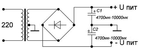
Bipolar power supply circuit
From the author:"The circuit is simple: a transformer, a diode bridge and a pair of capacitors. A transformer is needed in terms of power a little more than the total power of the channels, and capacitors - the more capacitance, the better. Only calculate the voltage of the windings so that the capacitors are no more than 50 volts."


The proposed scheme is designed to "power" integrated power amplifiers based on TDA7293 and TDA7294 microcircuits with the help of several external components. A distinctive feature of the proposed scheme is simplicity and lack of adjustment.
Many of those who assembled amplifiers on TDA7293 and TDA7294 microcircuits were faced with the fact that the real microcircuit does not hold the power declared in the Datasheet. One of the possible reasons is poor-quality Chinese microcircuits. However, they usually work well for a high-resistance load, from which we can conclude that the crystal simply overheats under load, and the vaunted thermal protection (as well as short-circuit protection) also works “in Chinese”: it does not protect against anything. A careful study of the microcircuit leads to the same conclusions - the ability of this case to divert more than 40-50w from the crystal is highly doubtful. Well, except to cool it with liquid nitrogen ...
Short circuit protection is also specific there - when working on a complex load (a real subwoofer), peak currents even at half power exceed the protection threshold, which causes a nasty crackle in the sound ... At the same time (a sad experience, alas) - after a couple of minutes, the microcircuit is still turns into a cloud of smoke, despite the best efforts of the internal protection circuit ...
And the very idea of TDA7293 and TDA7294 is very attractive - a small-sized module with a power of 100-130 W with a very decent sound (not high-end, but quite high-fi...). This is an amplifier for a home subwoofer, and an amplifier for a hybrid guitar apparatus, and 2-3 such modules with appropriate speakers are enough to sound small rooms ... It's a pity that it does not work, as the manufacturer's documentation promises ...
The idea to use the TDA7293 as a preamplifier with an external output stage was completely banal and obvious, and even reflected in the documentation for the microcircuit. The solution proposed by the manufacturer can be called simple with some stretch, and most importantly, it only reduces the power dissipated by the microcircuit, but does not increase the current delivered to the load ...
Therefore, it was decided to make the “help” in a different way, and, of course, as simple as possible. I’ll note right away that this solution is not in the audiophile style “only lamps and always in class “A”” ... No special measurement of distortion was carried out, but the circuit has no distortion visible on the screen and clearly audible to the naked ear, especially since the circuit was originally intended to work with subwoofer.
The input part is practically a typical TDA7293 inclusion. Slightly changed the circuit for generating control voltages on 9/10 pins of the microcircuit for simplicity. I will pay attention to the separate "grounds" of the input circuits and electrolytes for power and load! If you have a single-channel amplifier with a separate power supply and the signal is fed directly to the input of the TDA7293, then the grounds can not be separated (as is done on most printed circuit boards offered with the TDA7293). But if several channels are fed from one source, and even the signal comes from some kind of crossover, the “ground” of the power supply of which is also attached to the “ground” of the power amplifier, then questions arise like: “Why is it phoning? I shielded everything!” The track on the signet needs to be cut, and a 100 ohm SMD resistor can be soldered directly to the cut. The signal ground must be stretched with a separate wire (you can use a shielded wire screen) from the signal source. Since the external output stage operates in class B, to eliminate the “step” in the output signal, the resistor R8 is chosen to be relatively low-resistance (0.75 Ohm), and the highly linear TDA7293 works predominantly in the output current range up to 1 A. When the output current of the amplifier increases to about 1 A, the output transistor opens smoothly and the output current of the TDA7293 is limited by the sum of the base current of the output transistor and 1 A through R8. The value of R8 should not be further reduced - this will not noticeably increase linearity, and the power dissipated by the TDA7293 will increase. Capacitor C9 eliminates RF excitation and further reduces switching distortion of the output stage (more precisely, it allows the RF components from the TDA7293 output to go directly to the load, which quite effectively compensates for the "step" of the output pair of external transistors). In the first variant, one pair of output transistors was used, while the power at the resistive load equivalent of 4 ohms turned out to be 200 w sine when powered +/-55 v at idle. Under load, the power went down to about 48 v (power was supplied by a TC-360 transformer with a rewound secondary winding, filter capacitances were 15,000 microfarads each). Since the actual load is complex, a second pair of transistors and resistors R9 and R10 were added to improve reliability to equalize the currents between the pairs (if you need power less than 200 W, it is quite possible to limit yourself to one pair of output transistors. In this case, resistors R9 and R10 can be omitted). The feedback circuit is connected to the emitters VT1, VT2. This increases the output impedance of the amplifier by 0.08 ohms and, in my opinion, is not a defect. If the feedback is connected to the load, the output current of the TDA7293 will not be limited to 1 A, but will continue to grow, albeit slowly.
I recommend connecting acoustics through a relay with a connection delay circuit and protection against direct voltage at the output - the output stage does not have short circuit protection and in the event of any cataclysms there is a decent chance to damage the acoustics. In addition, on the free contact group of the same relay, I assembled a current limiter of the power transformer when turned on (a wire resistor of 100 ohms with a power of 10 W is included in the power supply circuit of the 220V transformer, closed by the free contacts of the relay) - an extremely useful thing with powers over 100 w. The usefulness of such a solution lies in the smooth increase in the supply voltage of the amplifier when turned on, and most importantly, in limiting the current from the network at the time of turning on. A further increase in power is quite possible: the allowable power supply for the TDA7293 is +/-60 v, the number of output transistors can be increased accordingly.
Everything that was said about the TDA7293 fully applies to the TDA7294 - taking into account the lower limiting supply voltage and a different scheme for connecting the voltage boost capacitor. My experience shows a slightly higher reliability of the TDA7294, but perhaps this is a consequence of the low-quality Chinese-made TDA7293 that have recently spread ... both current overload and voltage clipping - just attach an LED with a current-limiting resistor to the 5th output of the microcircuit, which is quite convenient.
The proposed solution - an external output stage - does not require tuning if assembled from serviceable components, because the quiescent current of the output transistors is 0. A serious drawback of the proposed circuit is the lack of protection against short circuits in the load - when an external output stage is connected, the built-in circuit does not work (fairness for the sake of it, it should be noted that the built-in circuit in the recommended inclusion never saved the microcircuit from burning out for me ...). However, if the proposed amplifier is built into, for example, a subwoofer, due to the lack of external connections to acoustics, the probability of a short circuit is negligible, and you can turn a blind eye to this drawback ...
It is possible to further reduce the power dissipated by the TDA7293 - increase R8, but this will inevitably increase the distortion introduced by the output stage (I believe that for use with a subwoofer, this is quite acceptable, especially since at low OOS frequencies, the microcircuits quite effectively compensates for them).
Structurally, it is convenient to mount the entire assembly directly on the heatsink - the microcircuit with the board is mounted in close proximity to a pair of output transistors (through mica gaskets and with the help of thermally conductive paste, of course), all elements except R8 and C9 are located on the microcircuit board, and
It is convenient to solder R8 and C9 directly to the terminals of the transistors.
This is what the layout of the variant with one output pair of transistors looked like:

Perhaps - a similar solution has already been proposed before - I did not conduct a “patent” search ...
List of radio elements
| Designation | Type | Denomination | Quantity | Note | Shop | My notepad |
|---|---|---|---|---|---|---|
| Audio amplifier | TDA7293 | 1 | Or TDA7294 | To notepad | ||
| VT1, VT3 | bipolar transistor | 2SC5200 | 2 | To notepad | ||
| VT2, VT4 | bipolar transistor | 2SA1943 | 2 | To notepad | ||
| R1 | Resistor | 33 kOhm | 1 | To notepad | ||
| R2 | Resistor | 680 ohm | 1 | To notepad | ||
| R3 | Resistor | 12 kOhm | 1 | To notepad | ||
| R4, R5 | Resistor | 33 kOhm | 2 | To notepad | ||
| R6 | Resistor | 47 kOhm | 1 | To notepad | ||
| R7 | Resistor | 100 ohm | 1 | To notepad | ||
| R8 | Resistor |
Hi all! In this article I will describe in detail how to make a cool amplifier for home or car. The amplifier is easy to assemble and set up, and has good sound quality. Below is a schematic diagram of the amplifier itself.

The circuit is made on transistors and has no scarce parts. The power supply of the amplifier is bipolar +/- 35 volts, with a load resistance of 4 ohms. When connecting an 8 ohm load, the power can be increased to +/- 42 volts.
Resistors R7, R8, R10, R11, R14 - 0.5 W; R12, R13 - 5W; the rest 0.25 W.
R15 trimmer 2-3 kOhm.
Transistors: Vt1, Vt2, Vt3, Vt5 - 2sc945 (usually c945 is written on the case).
Vt4, Vt7 - BD140 (Vt4 can be replaced by our Kt814).
Vt6 - BD139.
Vt8 - 2SA1943.
Vt9 - 2SC5200.
ATTENTION! The c945 transistors have different pinouts: ECB and EBK. Therefore, before soldering, you need to check with a multimeter.
The LED is ordinary, green, exactly GREEN! He's not here for beauty! And it should NOT be super bright. Well, the rest of the details can be seen in the diagram.
And so, let's go!
To make an amplifier, we need tools:
- soldering iron
-tin
- rosin (preferably liquid), but you can get by with the usual
- metal scissors
-cutters
-awl
- medical syringe, any
- drill 0.8-1 mm
- drill 1.5 mm
-drill (preferably some kind of mini drill)
-sandpaper
-and a multimeter.
Materials:
- one-sided textolite board measuring 10x6 cm
- sheet of notebook paper
-pen
- varnish for wood (preferably dark color)
- small container
-baking soda
-lemon acid
-salt.
I will not list the list of radio components, they can be seen on the diagram.
Step 1 We are preparing a fee
And so, we need to make a board. Since I don’t have a laser printer (I don’t have any at all), we will make the board “the old fashioned way”!
First you need to drill holes on the board for future parts. Who has a printer, just print this picture:

if not, then we need to transfer the markings for drilling to paper. How to do this you will understand in the photo below:

when you translate, do not forget about the fee! (10 by 6 cm)


something like that!
We cut off the size of the board we need with metal scissors.

Now we apply the sheet to the cut out board and fix it with adhesive tape so that it does not move out. Next, we take an awl and outline (by points) where we will drill.

Of course, you can do without an awl and drill right away, but the drill can move out!

Now you can start drilling. We drill holes 0.8 - 1 mm. As I said above: it is better to use a mini drill, since the drill is very thin and breaks easily. For example, I use a screwdriver motor.


Holes for transistors Vt8, Vt9 and for wires are drilled with a 1.5 mm drill. Now we need to clean our board with sandpaper.

Now we can start drawing our paths. We take a syringe, grind off a needle so that it is not sharp, we collect varnish and go!

It is better to trim the jambs when the varnish has already hardened.

Step 2 We charge a fee
For board etching, I use the simplest and cheapest method:
100 ml of peroxide, 4 teaspoons of citric acid and 2 teaspoons of salt.

We stir and immerse our board.


Next, we clean the varnish and it turns out like this!

It is advisable to immediately cover all the tracks with tin for the convenience of soldering parts.

Step 3 Soldering and tuning
It will be convenient to solder according to this picture (view from the side of the parts)

For convenience, from the beginning we solder all the small parts, resistors, etc.

And then everything else.

After soldering, the board must be washed from rosin. You can wash it with alcohol or acetone. On kraynyak it is possible even gasoline.

Now you can try to turn it on! With proper assembly, the amplifier works immediately. When you first turn on the resistor R15 must be turned in the direction of maximum resistance (we measure it with a device). Do not connect the column! The output transistors are MANDATORY on the radiator, through insulating gaskets.
And so: turn on the amplifier, the LED should be on, we measure the output voltage with a multimeter. There is no standing, so everything is fine.
Next, you need to set the quiescent current (75-90mA): to do this, close the input to ground, do not connect the load! On the multimeter, set the mode to 200mV and connect the probes to the collectors of the output transistors. (marked with red dots in the photo)
The amplifier is built on ThermalTrak series transistors from the well-known manufacturer On Semiconductor. These transistors are a new version of the top models MJL3281A and MJL1302A and have built-in diodes for thermally compensated bias circuits in the output stage.
As a result, adjustment of the quiescent current of the output stage is eliminated and there is no need for a classic voltage multiplier for thermal stabilization of the quiescent current of the output stage, and a number of design issues are solved to reduce the thermal resistance of the radiator-transistor.
The amplifier is made on a double-sided printed circuit board, although this would seem unnecessary for such a relatively simple design. However, the two-way wiring of the conductors allows you to optimize their location, in order to minimize mutual interference and compensate for magnetic fields created by the asymmetric currents of the class B push-pull output stage (we wrote about this in the series of articles "").
Features and Specifications
To begin with, a small note: in the description of their amplifier, the authors often mention either the “AB” mode or the “B” mode. In fact, the amplifier belongs to the class "AB", that is, at low signal levels it works in class "A", and at high powers it goes into class "B".
If in the first case (for small signals, class "A") the fight against magnetic fields and ripples in the power circuits does not present great difficulties due to the small values and symmetry of the currents, then when the amplifier passes to class "B", the currents become asymmetric and the intensity magnetic fields will be significant. It is somehow impractical to operate an amplifier with a maximum power of 200 W at levels of 3-5 W. Therefore, the authors paid special attention to obtaining maximum characteristics (and, accordingly, eliminating or compensating for all negative factors) at powers close to peak, that is, in the "B" mode.
The circuitry and design solutions used in the design made it possible to obtain:
- Very low distortion
- Lack of quiescent current regulation
- Double-sided printed circuit board with a simple topology of conductors
- Compensation of pickups of magnetic fields when working in class "B"
The main technical characteristics of the amplifier:
- Output power: 200W into 4 ohms; 135 W into 8 ohms,
- Frequency response (at 1 W): 4 Hz at -3 dB, 50 kHz at -1 dB
- Input voltage: 1.26 V at 135 W output power and 8 ohm load
- Input impedance: ~12 kOhm
- Harmonic distortion:< 0.008% в полосе 20 Гц-20 кГц (нагрузка 8 Ом); типовое значение < 0.001%
- Signal-to-noise ratio: less than 122 dB at 135 W power and 8 ohm load.
- Damping factor:<170 при нагрузке 8 Ом на частоте 100 Гц; <50 на частоте 10 кГц
Circuit Description
The figure shows a schematic diagram of a power amplifier:

Schematic diagram of the amplifier (click to enlarge)
The input signal through a 47 uF capacitor and a 100 ohm resistor is fed to the base of transistor Q1, a differential stage assembled from transistors Q1 and Q2. Low-noise transistors from Toshiba 2SA970 are used here, since it is this stage that makes the largest contribution to the final noise level of the entire amplifier.
The amplifier is covered by a common negative feedback loop, the values of the elements of which determine the gain. With the denominations indicated on the diagram, it is 24.5 times.
The capacitor in the negative feedback circuit provides 100% DC coupling to maintain zero potential at the output of the amplifier without the use of additional integrators, etc. With a capacitance of 220 uF, it provides a lower cutoff frequency of 1.4 Hz at a level of -3 dB.
Feedback Capacitors
The capacitances of the capacitors at the input and in the negative feedback circuit are somewhat larger than are usually installed in these circuits. Such values are chosen to minimize possible distortions in the audio frequency band.
For example, the output impedance of a CD player is typically several hundred ohms. If you install a capacitor with a capacitance of 2.2 μF at the input (typical value for input circuits), then at a frequency of 50 Hz the input stage will “see” the resistance of the signal source of the order of one and a half kilo-ohms. A 47 microfarad capacitor at the same frequency will have an impedance of only 67 ohms. (Recall that the signal source is essentially a voltage generator, so it must have a low output impedance)
Here also Not(usually recommended) non-polar capacitors are used. They are several times larger than simple electrolytic capacitors, which is why they tend to catch more noise and interference. Since the goal is to make an amplifier with a minimum level of noise and distortion, all measures have been taken for this: circuit design, choice of element base, design solutions.
The amplifier has a wide bandwidth, which also imposes its own requirements and restrictions on the choice of elements, installation, etc. in order to minimize the picked up noise and interference.
Diodes D1 and D2 protect the relatively low voltage electrolytic capacitor in the negative feedback circuit in the event of an amplifier failure. By the way, it is strongly recommended to equip the amplifier with some kind of speaker protection system. For the authors, it migrated from the previous design, so its description is not given here.
Using two diodes instead of one ensures that there is no harmonic distortion due to clipping of the signal peaks in the feedback circuit (about 1 V, and two diodes will give a limit of about 1.4 V).
Driver cascade
The main voltage amplification gives the cascade on the transistor Q9. To reduce non-linear distortion, the input stage is decoupled from the driver stage through an emitter follower on transistor Q8.
To obtain maximum linearity and maximum gain, the driver stage is loaded on an active current source (made on transistor Q7). The base bias for both it and the front end current source (Q5) creates transistor Q6. Several complex bias circuits of transistors Q5, Q6, Q7 provide maximum suppression of noise and ripple in the power circuits, which is important for a class “B” amplifier, where large (up to 9 A!) And, most importantly, unbalanced pulse currents walk along the power buses.
If the ripples of the power circuits get into the input stage, they will be amplified by all stages and fall into the load - the speaker system. What we hear as a result, most likely, we will not like. Therefore, the amplifier has taken all measures to prevent the penetration of noise and ripple from the power circuits into the amplifying path.
The oscillogram in the center shows a 1 kHz oscillator signal. The upper (red) graph is the modulation of the ripple of the positive power supply bus by the input signal, the lower graph is the modulation of the negative power bus:

A 100pF capacitor between Q9's collector and Q8's base limits the amplifier's bandwidth. Since the full amplitude of the output signal of the stage is applied to it, it must be rated for voltages of 100 V or more.
Output stage
The driver stage output on transistor Q9 is fed to the output stage transistors through 100 ohm resistors, which protect transistors Q7 and Q9 from a short circuit at the output of the amplifier, although, of course, the fuses should blow first. In addition, these resistors prevent possible excitation of the output stage.
The output stage is built on composite complementary Darlington transistors. Firstly, this made it possible to use high-linear ThermalTrak transistors with built-in diodes, and secondly, to get the maximum full power at a 4 Ohm load (to minimize the voltage drop at the output stage).
Offset Thermal Compensation
When using four Thermaltrak transistors in the output stage, we have four built-in diodes for organizing a thermally compensated bias circuit.
As shown in the diagram, four diodes are connected in series between the collectors of transistors Q7 and Q9. This method of organizing the bias of the output stage was widely used in the 60-70s. Later, it was replaced by the now classic transistor voltage multiplier.
Usually, the quiescent current of the output stage sets the stage on the transistor, which is mounted on the same heatsink with the output transistors, thereby providing thermal coupling. This method has disadvantages: firstly, the bias circuit transistor has to be selected to ensure optimal thermal compensation, and secondly, in any case, there is thermal inertia: the output transistor must heat the radiator, the radiator will heat the bias circuit transistor and only then will thermal compensation of the output stage current occur.
Placing diodes for thermal stabilization in the same package with a transistor solves these problems: diodes have characteristics that are as matched as possible with transistors, so thermal stabilization occurs as accurately as possible, secondly, they are located on the same substrate with transistor crystals, which makes them heating as quickly as possible, and an intermediary radiator is excluded.
With Thermaltrak transistors, thanks to the built-in diodes, the quiescent current of the amplifier quickly stabilizes after switching on and is maintained very accurately, regardless of changes in supply voltage or output signal level. The manufacturer also claims that the linearity of the cascade with such a bias is higher than when using a conventional transistor multiplier.
The figure explains how to set the output stage offset:

Four integrated diodes compensate for the four base-emitter junctions and determine the output stage current. Taking into account the fact that the output transistors are connected in parallel and 0.1 Ohm resistors are installed in the emitter circuits, four diodes connected in series provide the output stage quiescent current at the level of 70-100 mA, which is slightly higher than is usually set by the bias transistor node.
Output filter
The output filter is an RLC circuit consisting of a 6.8 mH inductance (without core), a 6.8 ohm resistor, and a 150 nF capacitor. This filter has been used by the authors in many amplifier designs and has proven to be highly effective in isolating the output stage from any reverse currents caused by a reactive load, thereby ensuring high amplifier stability. The filter also effectively suppresses RF signals picked up by long speaker wires, preventing them from entering the amplifier's input circuits.
Circuit breakers
The output stage is fed by 5A fuses from the ±55V rails. These provide the amplifier's sole protection against output short circuits or other faults that result in excessive current draw.
Double-sided PCB
To simplify and optimize wiring power circuits The printed circuit board of the amplifier is double-sided. Firstly, this made it possible to organize the wiring of the common wire in the form of a "star", when all conductors with zero potential converge to one point, which eliminates the formation of "earth" loops and the penetration of the output signal into the input circuits. We wrote about this in a series of articles ""
Secondly, and more importantly, the wiring and layout on the board is designed to compensate for the magnetic fields created by high surge currents. We also wrote about this in the series of articles "", where it was proposed to twist bifilar conductors with large and antiphase currents. On a printed circuit board, conductors cannot be laid like that, but it is nevertheless possible to compensate for the fields.

For example, the positive power rail fuse is located side by side and parallel with output stage emitter resistors Q12 and Q13. The elements are connected so that the current flows through them in different directions, due to which the mutual compensation of magnetic fields occurs. Similarly, the details are placed on the negative bus.
The power paths from the CON2 connector to the fuses run side by side parallel to each other, and in the middle of the board they diverge in different directions. Under the diverging conductors are the tracks of the emitter circuits of the output stage, and under the parallel tracks are the ground bus. Due to this layout of the printed circuit board, the magnetic fields created by these tracks are mutually compensated.
The applied methods of suppressing magnetic fields made it possible to significantly reduce the distortion of the amplifier.
The results of measurements of the parameters of the amplifier:

Frequency response of the amplifier at an output power of 1 W at a load of 8 ohms

Harmonic distortion of the amplifier at a frequency of 1 kHz with a load of 8 ohms. It can be seen that clipping occurs at a power of 135 watts.

Harmonic distortion of the amplifier at a frequency of 1 kHz with a load of 4 ohms. It can be seen that clipping occurs at a power of 200 watts.

Amplifier distortion into 8 ohms (resistive load)

Amplifier distortion at an output power of 100 watts into a 4 ohm resistive load.
To be continued...
The article was prepared based on the materials of the journal "Practical Electronics Every Day"
Free translation: Chief editor « »
We also recommend
 Soldering iron or blow dryer?
 Compact multifunctional instrument - L, C, ESR meter, probe-signal generator
 Transistor KT815: parameters, pinout and analogues Transistor KT 815 technical specifications
 Simple PCB Drilling Machine Small PCB Drilling Machine
 Power supplies for ULF circuits and seals
 Feedback Capacitors